This is a tutorial for
HobECAD.
HobECAD Tutorial
HobECAD is a schematic capture and printed
circuit board (PCB) editing system that is
capable of generating industry standard RS274X
(i.e. Gerber) files that can be manufactured
by a wide variety of PCB manufacturers. It
currently runs on Linux under the X11 window
system. HobECAD is designed to be a fairly
minimal system that has a relatively low
learning curve that is suitable for electronics
hobbyists.
This document is a tutorial which will introduce
you to the HobECAD system. The project that has
been selected is a small hobby level digital logic
probe. This probe will light a red LED (Light
Emitting Diode) if it detects logic "low" and
a green LED for logic "high". Neither the red nor
green LED's will light up if no logic voltage is
present. Indeed, this is a useful enough project
that I will probably have it shipped off to be
manufactured.
The steps involved in using HobECAD are outlined below:
-
Downloading and Installing
-
The is covered in the
HobECAD Download and Installation
documentation. It is not covered in
this tutorial.
-
Setting Things Up
-
HobECAD works best when all of the
files are structured into directories
and sub-directories. Rather than ask
you to figure this out on your own,
I will describe the basic set up that
I use. Once you understand it, you are
welcome to go off on your own and change
things around (or not) to your satisfaction.
-
Schematic Capture
-
Schematic capture is the process of drawing
your circuit using fairly typical electrical
symbols. This schematic is later used to
verify that the printed circuit board is
properly layed out.
-
Parts Management
-
HobECAD uses a standard text editor to manage
parts and packages. Once the parts and
packages have been entered, hobecad
can detect some improper electrical wiring
in the schematic(s) (e.g. shorting Vcc and
ground, two logic gate outputs tied together,
etc.)
-
Printed Circuit Board Layout
-
After all of the parts have been entered
into their various text file formats, it
is possible to start laying out the printed
circuit board using hobecad.
-
Verification
-
Verification is the process of determining
where the printed circuit board design
and the schemtic(s) differ and then correcting
either the printed circuit board or the
schematic(s) to bring them into allignment.
Finally, the various layers of the printed
circuit board are viewed with gerber
utility for viewing RS274X (Gerber) files.
-
Manufacture
-
Lastly, the various RS274X files are gathered
together into a
.zip file and
shipped off to a PCB manufacturer for
manufacturing.
With the exception of downloading and installing,
I will cover each of these topics in the sections
to follow.
Over the years, I have learned to organize my
projects that use HobECAD into directories and
sub-directories. The top level directory is
typically a project directory. If the project
consists of more than one board, each board
gets its own sub-directory. It is extremely
rare to get a board right on the first run,
I usually have a sub-directory for each revision.
This is shown in outline form below:
-
Project/
-
Board_1/
-
Revision_A/
-
Revision_B/
-
...
-
Board_2/
-
Revision_A/
-
Revision_B/
-
...
-
...
If the project only consists of one board, the
board sub-directories are compressed out the
the file hiearchy.
In addition to the directory structure I use a
program called make to run the the
various programs of the HobECAD system.
The make program is by no means a
favoriate of mine, but it seems to get the job
done. Thus, each file in each directory will
have a Makefile file that contains
instructions for building things in that
directory.
In addition, there are a number of files that
that are shared across all of the boards and
revisions that live up in the top-level project
directory. The most important of theses is a
file called Makefile_share.mk.
This file contains a bunch of rules that direct
make in the running of hobecad.
Lastly, the top-level directory also contains
some part management files that are shared
amongst all of the boards and their revisions.
These files have suffixes of .prt
and .pkg.
Now it is time to set things up to use HobECAD:
-
Create a project directory:
	prompt$ cd .../somewhere
	prompt$ mkdir myproject
	prompt$ cd myproject
where somewhere is the location on your
file system where you have decided to set up
you project and myproject is the name
you have given your project.
-
For starters, we will assume that your project
only needs one board. Thus, we will skip
setting up per board sub-directories.
-
Now we will create the first revision directory.
To save typing, the revision sub-directory is
called
rev_a is in all lower case.
prompt$ mkdir rev_a
-
Now it is time to grab the
Makefile_share.mk file and
install it in the top level directory.
prompt$ cp .../hobecad/example.Makefile_share.mk .
where .../hobecad is the path
to the hobecad directory you unpacked HobECAD
into.
-
You need to create you top level
Makefile. Using your favorite
text editor, create a Makefile
that looks basically like this:
	all:
		cd rev_a; $(MAKE)

	clean:
		cd rev_a; $(MAKE) clean
It is extremely important that the lines that
start with cd rev_a; ... start
with a tab characters; spaces will not work.
Make is one of the few programs out there that
cares about spaces vs. tabs. The make
program basically insists that the file be
named Makefile.
-
We need to create our empty parts and package
files.
	prompt$ touch myproject.pkg
	prompt$ touch myproject.prt
These files will be filled in later on.
-
Now we can go down into the revision A directory
and set it up.
prompt$ cd rev_a
-
We need to make another
Makefile
in the rev_a directory. Make its
contents look as follows:
	BASE := myproject
	SC_BASES := $(BASE)

	include ../Makefile_share.mk
-
We need to start the parts list file:
prompt$ touch myproject.ptl
It starts out empty and we will fill it in
later on.
As a final comment, you are welcome and encouraged
to store additional project information into these
directories. For example, if you are using a
microcontroller, the source code for your
microcontroller should live in the same directory.
Likewise, any documentation or specifications
can also be stored there. In addition, I tend
to do all of my projects so that they can be
viewed via the web, so all of my HTML (HyperText
Markup Language) files live in the same directory
structure. Since none of these files are directly
related to learning HobECAD, they have been omitted
from this tutorial.
Now it is time to enter a schematic for the
digital logic probe.
Before starting the schematic, it is useful to
have a short discussion of "Why?" There are
three important reasons for doing a schematic.
First, it provides a human readable diagram
of the circuit. Second, it is possible to get
HobECAD to verify that the printed circuit
board exactly matches the schematic(s). Thus,
when you are debugging the circuit, there is
high confidence that the schematic actually
matches the circuit you are debugging. The third
reason is because HobECAD can do a little
signal checking to verify things like there is
no short between ground and Vcc and the like.
In addition to helping you create the circuit
schematic, the hobecad program reads
the circuit schematic(s) and generates a wire
list that describes which leads of what components
are attached to one another. In addition,
The hobecad program can also read the
printed circuit board and extract a wire list.
Since both lists are generated in alphabetical
order, the standard Unix style diff
program can high light the differences between
the two wire lists. When there are no differences
between the two lists, the user has high
confidence that the printed circuit board
implements the schematic(s).
Now that I have explained why you should have a
schematic, it is time to actually use hobecad
to create one. The project I have selected is an
inexpensive digital logic probe. Please follow the
following steps:
-
Start hobecad as follows:
prompt$ hobecad -c 10 myproject.sc
The -c 10 tells HobECAD to use
10 pixel square cells. The .sc
tells HobECAD to go into schematic
capture mode.
-
After you start hobecad, you are
presented with a white window with a small
black square in the lower left corner. That
small black square is the cursor. The cursor
can be moved by clicking on the left mouse
button over the location you want to move
the cursor to. The cursor color can be toggled
between black and brown by clicking on the
middle mouse button. Lastly, the thickness
of the cursor can be changed by clicking
on the right button. Please experiment
a little by clicking on all three buttons.
Do not worry if you accidently draw any lines.
-
To exit without saving anything,
click on the the little `X' on the top
most row of the window. Please do so,
right now. Please note that it immediately
exits without giving you a chance to change
your mind. It typically displays an error
message of the form:
X connection to :0.0 broken (explicit kill or server shutdown).
This message is OK; please do not worry about it.
When you click on the `X', editing immediately
terminates, any edits you have done are lost
forever, and they can not be recovered.
(No, this is not considered to be good user
interface design, but it is what hobecad
does.)
-
If you do a directory listing, there will
be no file named
proble.sc
because you exicted without saving.
	prompt$ ls
	{directory listing here}
-
Let's restart hobecad:
prompt$ hobecad -c 10 probe.sc
Again, we are presented with a blank
white windows with a black square in
the lower left corner. We are back
to where we stared. Cool.
-
Now this time, let's exit hobecad
and save the file contents. This is done by
depressing the [Esc] key (typically in the
upper left hand side of the keyboard.)
Please depress the [Esc} key now. Notice
that the window disappears and there is no
confusing message from the window system.
If you do a directory listing, you will
find that the file
probe.sc
now exits.
-
You now know how to start editing with
hobecad and two ways of leaving
hobecad ([Esc] and `X'.)
-
Now it is time to do some actual editing.
Restart hobecad on
probe.sc:
prompt$ hobecad probe.sc
You will note that this time the -c 10
option is not specified. This is because the
file remembers its cell size when it written
out. It may be tempting to try to edit
schematics at a different cell size, but frankly
there are too many bugs for that to work;
so please do all schematics at a cell size
of 10.
-
Now we are going to enter some text.
Please click the middle mouse button to
change the cursor color to brown and
type the following:
Copyright (c) 2002 by First M. Last
where First M. Last is your first name,
middle initial, and last name. (Actually,
nobody really cares what name you use, so you
can be creative here.) As you type in each
letter it, the cursor advances one cell to the
right. Upper case letters are bold and
lower case letters are shown as non-bold
upper case letters. There is a good case
the text does not fit in the square window.
You can resize the window by grabbing any
corner with the left mouse button and
resizing the window. Now using the mouse,
position the cursor above the first line
(use left mouse button), change the cursor
color (use middle mouse button) to brown,
and type:
Digital Logic Probe (Rev. A)
The resulting screen should look as shown
below:
with the exception of the mark in the upper
right and corner (please ignore the artifact
for now; it is just a way to trick the software
into drawing the window at a reasonable size.)
If the characters are black, you should delete
them (see next paragraph) and switch them over
to brown.
-
When typing in text, you can use the [Del]
key to delete the character to the left of
the cursor. Indeed you can insert charcters
into the middle of the string using the mouse
to click the cursor to the desired insertion
point. Likewise, you can delete characters
in the middle of the string. For example,
replace your middle initial with your full
middle name and delete the characters back.
-
You now know how to insert and delete characters.
It is always a good idea to but some information
on the schematic that specifies what it is
(i.e. a digital logic probe), what revision
(i.e. revision A), when it was edited (i.e. 2002),
who the creator is (i.e. you), and some sort
of copyright notice. This information is
completely optional in the sense that
hobecad will process the file
irrespective of whether or not the information
is present or not; however it is still a good
idea enter the information.
-
Now it is time to explain the purpose of the
colors. With exactly one exception that
is dicussed shortly, anything in brown is
completely ignored by hobecad
when it is reading your schematics. Anything
entered in black is used by hobecad
when it processing the schematic.
-
The subject of glyphs is introduced next.
A glyph is basically an electronic symbol
that has been preentered into the HobECAD
symbol library. The various glyphs in the
HobECAD glyph library can be found in the
HobECAD documentation.
-
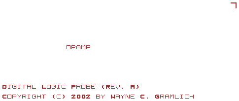
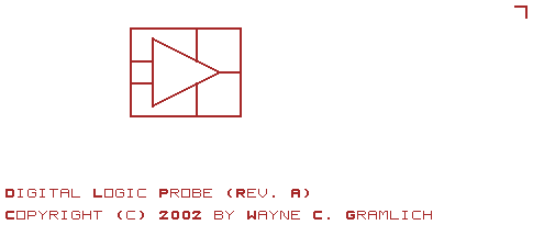
We are going to draw an operation amplifier
(i.e. an opamp) into our schematic in the
brown layer. Please move the cursor to
approximately the center of the drawing area
using the mouse, make sure the cursor is
brown, and then type (in lower case):
opamp
the resulting screen should look as follows:
-
Now, with the cursor sitting somewhere on
the word
opamp, depress the
[Control-X] key. This key code is generated
by holding down one of the keys on the
keyboard labeld [Control] or [Cntrl] and
then depressing the [X] key while still
holding the [Control] key down. There
is no need to touch the [Shift] key. When
you do this, an operational amplifier symbol
shows up pointing down. It should look as
follows:
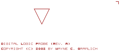
Notice that the text that spelled out
opamp has been removed.
-
The [Control-X] key is used to insert
a glyph into the drawing. It is done
by typing the name of the glyph followed
by typing the [Control-X] key. As far
as HobECAD is concerned, the glyph is
located where the first character of
the glyph name used to be. There is
no visible locator for the glyph location
other than the glyph itself.
-
The [Control-D] key is used to delete a
glyph. This is done by placing the cursor
over exactly the glyph is located and
typing [Control-D]. This causes the
glyph to be deleted and we are back we
we started.
-
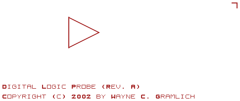
Each glyph can be oriented in one of four
directions - left, up, right, and down.
If you just type in the glyph name,
you get the down orientation. If you
follow the glyph name with the character
'<', '^', or '>', you get the left, up,
and down orientations of the glyph.
Please type in:
opamp>
followed by typing [Control-X]. You should
wind up with the operation amplifier symbol
pointing to the right as shown below:
-
You now know how to insert and delete glyphs
using hobecad.
-
Next, we will learn how to draw lines. By
the way, there isn't much more to the
hobecad editor other text, glyphs,
and lines.
-
Lines are drawn and erased using the mouse.
A line is started by clicking the with
left mouse where you want to start the line.
Next, leaving the left mouse button depressed,
the mouse is dragged to where the end point
of the line is to be. hobecad will
only draw lines that are vertical, horizontal,
or at a 45-degree diagonal. Lines are erased
by retracing the line.
-
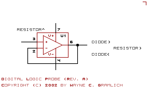
Using the thin brown cursor, please draw a
box around the operational amplifiere along
with lines for the inputs, outputs, and
power supplies. It should look as shown
below:
-
Now we are going add a bunch of labels.
The labels will identify the pin numbers
for a common LM741 operational amplifier.
We add labels inside of the box for the
inverting (-) and non-inverting inputs
(+) as well as the positive and negative
power supply leads (V+) and (V-). These
labels are done in brown. The pin numbers
are done outside of the box in black
(use the middle mouse button to change
colors.) The user label for the op amp
(U1) is done in black inside of the brown
box.
-
In HobECAD schematics, a brown box is with
a single black label is the only time where
brown is recognized as part of the schematic.
This is a component box, and the black label
is the component label. The black numbers
outside of the box are the component leads
and they can be numbers, letters, or other
characters such as plus (+) or minus (-).
-
Now we are going to draw our first wires in
black now. Black lines represent always
represent signal wires. Please add some
black wires that look as follows:
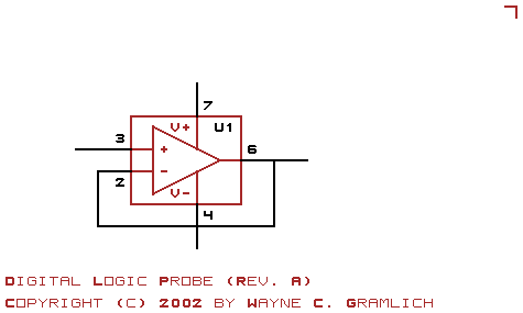
Whenever a black wire terminates on the
side of brown box, hobecad looks
for a black label that identifies which
lead is being connected to. hobecad
will get confused if it sees no black label
or two black labels and will generate an
error message when the wire list is extracted.
-
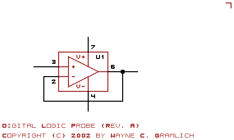
We need to indicate where two wires connect
by adding a connection dot. This is done
using the mouse. Place the black cursor
over the connection point, depress and hold
down the left mouse button, now click the
middle button and a black connection dot will
appear. To erase the connection dot,
just do the same operation again. Your
schematic should look as follows:
-
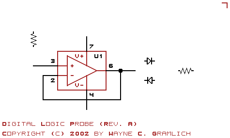
Now it is time to add a couple of light
emitting diodes and couple of resistors.
The resistor glyph is called
resistor and the diode
glyph is called diode.
The glyphs are entered in black at the
approximte locations shown below:
And after you type [Control-X] over each
piece of text, you get the following:
And after some black wires and connections
have been added and some brown diagonal
lines to indicate light emitting diodes
you should have the following:
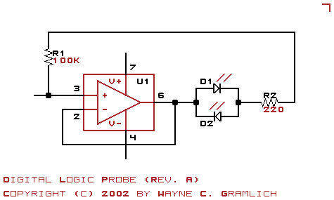
The black labels identify the components
and for resistors and the diodes, hobecad
"knows" what the leads are named. For
resistors, the leads are named "A" and "B"
and for diodes they are named "+" and "-".
Lastly, the "100K" and "220" specify the
resistor value in ohms in brown.
-
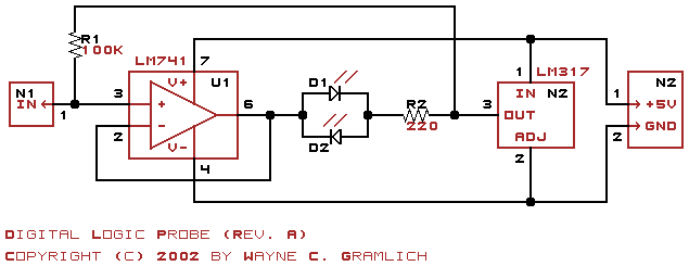
We are on the final stretch now. Let's
add the 1.25 volt regulator (the LM317),
the input probe (N1), and the voltage
input terminals (N2). The resulting
diagram should look as follows:
There are additional features in HobECAD, but
you have seen most of them by now. It should
be possible to go back and read the
HobECAD documentation to discover the
remaining minor features (cut and paste.)
I need to give a few definitions here before we
can get into the parts managment topic very deeply.
-
Component/Part
-
A component or part is an electronic part
that performs a particular function -- e.g.
a resistor, a capacitor, a transistor,
a diode, an integrated circuit, etc.
-
Package
-
A package is the way a component is
packaged up use in an electronic
circuit. Many different components
use the same package. For example,
many integrated circuits come in
the DIP-14 (Dual Inline Package -
14 pins.) Some components are
alternatively in a TO-220 or a TO-92
package.
-
Lead
-
A lead is one wire connected to package.
It can be used for signals or power.
A DIP-14 has 14 leads, a TO-220 has
3 leads, etc.
-
Parts List/Bill of Materials
-
A parts list assigns a short name to each
part used by a given board.
Hopefully, these definitions are pretty intuitive.
The purpose of parts management is to keep HobECAD
informed about about the relationship between the
parts list, schematic, and printed circuit board
layout. The symbols in a schematic identify parts
in the parts list. The printed circuit board
layout needs to know about where the various leads
of a component on a board are located. Eventually,
HobECAD can scan through a parts list, and generate
a corresponding list of vendors, part numbers and
costs.
When designing HobECAD, I could not come up with
a particularly compelling reason create a fancy
graphical user interface for managing parts
information. Instead, everything is kept in
flat ASCII text files. Yeah, it is boring, but
it is fairly simple to learn and manage. There
are three file formats:
-
Parts List (
.ptl) -
The parts list makes an association between
a symbol name on the schematic (e.g. N1,
Q2, R3, U4, SW1, etc.) and a part
(e.g. 74LS00, LM741, NE555, PN2222, etc.)
Optionally, a suggested vendor and part
number can be provided. A parts list
file and schematic should be enough for
somebody who is really dedicated to duplicate
a circuit. This is exactly one parts list
file per printed circuit board.
-
Part/Component Catalog (
.prt-
A component catalog list a bunch of parts
that can be used in a project. Each
entry specifies the component name,
(e.g. 74LS00) the corresponding package
that the omponent uses (e.g. DIP14),
and a list of leads used in the package.
(The lead list is discussed in greater
detail later.) In addition, it is
possible to optionally specify what
a vendor, vendor part number, and
vendor pricing information. More than
one vendor may be listed in a single
part/component catalog. In addition,
multiple catalogs can referenced by
a single printed circuit board design.
-
Package Catalog (
.pkg) -
A package catalog lists a bunch of
different package names and the
corresponding placement of the pins
on a printed circuit board. Each
entry consists of a package name
(e.g. TIP31) and a list of leads.
Each lead has a name (e.g. E, +, 1)
and an X Y position relative to
one pin which is designated as the
pivot pin that the package can be
turned about.
All of the file formats use a similar format.
First, blank lines are ignored as are any lines
that start with a `#'. There are no continuation
lines.
Below is the parts list file for the digital logic
probe (probe.ptl):
    # Digital Logic Probe (Revision A):
    #
    D1-2: LSG2040 - Green LED [Jameco: 34606]
    N1: Probe_Wire - Probe wire
    N2: Terminal2.Probe - 2 Junction Terminal Strip [Jameco: 189675]
    R1: 100K_Resistor - 100K Ohm 1/4 Watt resistor [Jameco: 29997]
    R2: 47_Resistor - 47 Ohm 1/4 Watt resistor [Jameco: 31106]
    U1: LM741 - Operational Amplifier [Jameco: 24539]
    U2: LM317LZ - Positive Voltage Regulator [Jameco: 23552]
The first two lines are comments. It is useful to
put the project name and revision information in
a comment. Symbol names are constrained to be
a sequence of upper case letters followed by a
decimal number. If there is a range of parts,
this is specified by add a dash followed by the
last number in the range. The colon is required.
The part name is a a sequence of upper and lower
case printing letters with no spaces. Each part
name must exactly match one listed in part catalog
file. The part name is followed by a hyphen.
Everything between the hyphen and optional
opening square bracket is a comment and is
ignored by HobECAD. A vendor and part number
is specified by enclosing the vendor name and
part number in square brackets separated by
a colon. Everything after the hyphen is
optional.
I should mention that there is a bug in HobECAD where
it does not complain about extra parts in the parts
list. One of these days I will track that down and
fix it.
The next file to look at is the part catalog file.
The part catalog file for the probe is reproduced
below:
    # Digital Logic Probe Part Catalog:
    #

    H Parts 1 0

    P LSG2040 LED1 - Green LED [Jameco:34606;LEDs $.15/10 $.13/100]
    L + + Other
    L - - Other

    P Probe_Wire Wire - Probe wire
    L 1 1 Other

    P Terminal2.Probe TerminalStrip2 - 2 Junction Terminal Strip [Jameco:189675;Connectors $.69/1 $.62/10]
    L 1 1 Other
    L 2 2 Other

    P 100K_Resistor Resistor4 - 100K 1/4 Ohm Resistor [Jameco:29997;Resistors $.99/100]
    L A A Other
    L B B Other

    P 47_Resistor Resistor4 - 47 1/4 Ohm Resistor [Jameco:31106;Resistors $.99/100]
    L A A Other
    L B B Other

    P LM741 DIP8 - Operation Amplifier [Jameco:24539;ICs $.29/1 $.25/10]
    L 1 OFFSET_NULL1 Other
    L 2 V- Other
    L 3 V+ Other
    L 4 GND Other
    L 5 VOUT Other
    L 6 OFFSET_NULL2 Other
    L 7 VCC Other
    L 8 NC No_Connection

    P LM317LZ TO92 - Low voltage regulator [Jameco: 25532;ICs $.49/1 $.39/10]
    L 1 VIN Other
    L 2 VADJ Other
    L 3 VOUT Other
As usual, blank lines and lines that start with a `#'
are ignored. A comment at the beginning to explain
roughly what is inside is appropriate. The line
H Parts 1 0
specifies that it is a parts catalog file. We will now
dissect the following part line:
P 100K_Resistor Resistor4 - 100K 1/4 Ohm Resistor [Jameco:29997;Resistors $.99/100]
Each part is identified by a line that starts with
capital `P', followed by the part name
(100K_Resistor'), followed by a package
name (`Resistor4'). Next comes the comment
which is a hypen (`-') followed by some
uninterpreted text. The comment is terminated by either an
end of line or an opening square bracket (`[').
The optional vendor inforation is contained in the square
brackets (`[ ... ]'). There is
a vendor name (`Jameco'), followed by a colon
(`:'), followed by a part number
(`29997'), followed by an optional
semicolon (`;') and a correspondingly
optional catalog section name (`Resistors').
Lastly, there is optional pricing information of the
form of a price (`$.99'), a slash
(`/'), and a quantity (`100').
There can be multiple price and quantity pair specified
separated by one or more spaces.
The part number in the part catalog file
(.prt.ptl). If they do
not match, an error message is generated.
When HobECAD is being used to generate a final parts
list, it sorts all of the required parts by vendor
name first, followed by vendor catalog section name,
followed by vendor part number. Thus, all of the
parts that came from the same catalog section will
be grouped together in the parts list. This can
simplify parts ordering over the phone. In addition,
sometimes it is more cost effective to order more
parts than you actually need to get a price break.
The HobECAD software will make a recommended quantity
as well.
The example above does not show fractional parts.
Sometimes it is appropriate to purchase a part
that can be broken into smaller parts. For example,
a 2×40 male header can be broken into smaller
pieces (e.g. 2×5, 2×13, etc.) The fractional
part is specified by putting a fraction number before
the vendor name (e.g. `10/80'). The
HobECAD software will add up all of the fractional
pieces and figure how many of the whole pieces are
needed.
After the part name, comes the lead lines. Each
lead on the part gets a lead line. A lead line
looks as follows:
L package_lead_name part_lead_name signal_type
where
-
package_lead_name
-
The package lead name is the name of the
lead in package catalog file (
.pkg.)
-
part_lead_name
-
The part lead name is the name that
part specification sheet uses to describe
the lead (e.g. Vin, D, Q, CLK,
etc.)
-
signal_type
-
The signal type specifies the type of the signal.
The signal type is one of:
-
Ground -
The lead is attached to ground.
-
Vcc -
The lead is attached to +5 volts.
-
TTL_In -
The lead is a TTL input lead.
-
TTL_Out -
The lead is a TTL output lead.
-
TTL_Tri_State -
The lead is a TTL Tri-state lead.
-
Other -
The lead is some other lead.
The HobECAD software will verify that there
are not accidental shorts between ground and
Vcc, no two TTL outputs are tied together etc.
The package catalog file (.pkg) for
the digital logic probe looks as follows:
  # Digital Logic Probe Packages:

  H Packages 1 0

  P Wire - A wire for probe tip
  L 0 0 1*

  P TerminalStrip2 - 2 Junction Terminal Strip with .2" between leads
  L 0 0 1*
  L 0 4 2

  P LED1 - LED with .1" between leads
  L 0 0 +*
  L 0 2 -

  P Resistor4 - Resistor with .4" between leads
  L 0 0 A*
  L 0 6 B

  P TO92 - TO92 3 lead package splayed into a "V" with pin 2 pointing down
  L 0 2 1
  L 1 0 2*
  L 2 2 3
As usual, the package catalog file ignores lines that
are blank or starts with a (`#'). The line
H Packages 1 0
specifies that the file is a package catalog file.
Each part is specified by a line that starts with
a P, followed by a package name,
followed by a hyphen (`-'), followed
by an uninterpreted comment.
After each package line is a list of lead lines.
Each lead line has the following form:
L x y name
where
-
x
-
The X coordinate of the lead in units of
.05 inch.
-
y
-
The Y coordiante of the lead in units of
.05 inch.
-
name
-
The lead name.
One of the leads must marked with a trailing
asterik (`*') to mark which
pin on the package is pivoted when the package
is reorient on a printed circuit board.
The package is always entered into the
package catalog file in a pointing down
orientation.
Now once you have entered in the three files
(.ptl, .prt, and
.pkgMakefile has been set up
so that all you have to do is type:
make
and it will run hobecad with the
appropriate arguments. The command it runs is:
hobecad -C -w probe_sc.wl probe.sc probe.ptl ../probe.prt ../probe.pkg
The -C option turns on checking.
The -w probe_sc.wl causes the file
wire list file probe_sc.wl to be
generated from reading the schematic. The
digital logic probe only consists of a single
schematic -- probe.sc. In addition,
the parts list file (probe.ptl),
the parts catalog file (probe.prt),
and the package catalog file (probe.pkg).
In addition, the files hobecad.prt
and hobecad.pkg are read from the
same directory that contains the hobecad
executable. The file hobecad.pkg
contains the definition for the DIP8 package.
The resulting wire list file (probe_sc.wl)
looks as follows:
    D1:+ D2:- U1:2 U1:6
    D1:- D2:+ R2:B
    N1:1 R1:B U1:3
    N2:1 U1:7 U2:1
    N2:2 U1:4 U2:2
    R1:A R2:A U2:3
Each line in the wire list file corresponds to a
single `wire' that interconnects two or more
leads on various components. For example the
first line says that D1:+ is
connected to D2:-, U1:2,
and U1:6. The lines in a wire list
file are sorted alphabetically (e.g.
D1:+, D1:-,
N1:1, N2:1,
N2:2, R1:A.)
On a given line, all of the leads are sorted
alphabetically (e.g. N1:1,
R1:B, U1:3.)
When the wire list is extracted from the
printed circuit board layout, it will be
sorted in exactly the same way. The net
result is that when the wire lists exactly
match on a character by character basis,
the printed circuit board layout matches
the schematic.
Now it is time to dig into the layout of a
printed circuit board.
-
Now it is time to create the printed circuit board:
prompt$ hobecad probe.pcb
This brings up a window that can be used to
edit the probe printed circuit board.
-
HobECAD currently restricts printed circuit boards
to three layers -- red (back copper), green (front
copper) and black (silk screen artwork.)
-
The left mouse button is used to draw and
erase lines, the middle mouse button is used
to change layers, and the right button is used
to change line thickness between thick and thin.
You are free to use the [Control-L] (change
layer) and [Control-T] (toggle thickness) keys
instead of the mouse button. A via or component
hole is dropped by holding down the left clicking
the middle button. Alternatively, the [Control-V]
or [Control-P] key may be used.
-
{more tutorial goes here}.
-
Once you have your printed circuit board:
	prompt$ make
	{a bunch of stuff here}
Now you should have the printed circuit board
wire list in the file
myproject_pcb.wl.
-
Now edit the
Makefile and add the
following line to the end:
all: $(BASE).diff
-
Re-run make:
	prompt$ make
	diff myproject_sc.wl myproject_pcb.lwl
	{differences listedhere}
If there are any differencs between the two wire
lists there is either a mistake in the schematic
or a mistake in the printed circuit board design.
The differences should help to figure what is
wrong.
-
Once the mistakes have been corrected,
It is time to edit the
all:
line in the Makefile to look
as follows:
all: $(BASE).diff ${GERBERS} ${PNGS} $(BASE).parts
-
Now run make:
	prompt$ make
	{stuff here}}
This causes the generation of the gerber files,
the generated image files in PNG file format, and
the parts list file.
-
Edit the
all: line in
Makefile to also contain
$(BASE).zip:
all: $(BASE).diff ${GERBERS} ${PNGS} $(BASE).parts $(BASE).zip
-
Now run make:
	prompt$ make
	{Generate zip file}
This generates the zip file needed to be sent off to
the printed circuit board vendor.
Copyright (c) 2002 by
Wayne Gramlich All rights reserved.