This is the documentation for the
HobECAD is an ECAD (Electronic Computer Aided
Design) system for the electronics hobbiest.
HobECAD Documenation
Both the schematic capture and printed circuit board
layout are implemented by the same drawing program
called HobECAD. The HobECAD program
basically implements a grid on which you can draw
special symbols, text, and either thick or thin lines
that are constrained to be horizontal, vertical, or
diagonal.
For now, everything in is controled via the keyboard and
mouse; there are no screen buttons or controls. (The
eventual solution to this problem is to upgrade to a
window toolkit that supplies buttons and controls.)
There are two modes that hobecad can be
operated in; the two modes are:
-
Schematic Capture Mode
-
Schematic capture mode is entered by
specifying a suffix of .sc on the file
name when it is created. In schematic
capture mode, there are two layers that
you can draw into; the two layers are:
-
Wire Layer (black):
-
The wire level uses lines to represent
wires that interconnect electrical
components. This layer is also used
to label the pins of components.
-
Component (brown):
-
The component layer is used to represent
the components of the circuit. Since
some components are basically represented
by a box with some text inside, drawing
these lines in a different layer
distinguishes them from wires.
When a schematic is printed out to a printer,
all layers will be printed in a single color
(black). The reason for keeping the component
and wire layers separate is because the
consistency checker needs a way to distinguish
between lines the represent wires interconnecting
components and lines that are used represent
integrated circuits (e.g. flip-flops, counters,
etc.)
-
Printed Circuit Board Layout Mode
-
PCB layout mode is entered by specifying a
suffix of .pcb on the file name when starting
HobECAD. In PCB layout mode, there
are three layers that you can draw into; the
three layers are:
-
Front (green):
-
This layer corresponds to the front
(component side) copper layer on a
printed circuit board. If you are
laying out a single sided printed
circuit board, the front layer is
not used.
-
Back (red):
-
This layer corresponds to the back
(solder side) copper layer on a
printed circuit board.
-
Artwork (black):
-
This layer corresponds to the black
artwork that is frequently applied
to the component side of the printed
circuit board to aid in component
placement.
Other than the number and color of the layers, the
HobECAD program behaves the same in both
schematic capture and printed circuit board layer
mode.
The reason for using a .05 inch grid, rather than the
much more sensible metric system, is because .1 inch
is the most common spacing between pins on a integrated
circuit in a dual in-line package (DIP).
The hobecad command line options are:
-
-c cell_size
-
The cell_size can be either 10 or 15
pixels square at the moment. 15 is the
default cell size.
-
-d mono|gray|color
-
Force the display into monochrom, grey scale,
or color mode. Do not use this option.
-
-D
-
This causes HobECAD to write out
any files in debug format. Debug format
stores all symbols in absolute coordinates
rather than relative coordinates. For
someone who understnads the file format,
it is possible to grep for symbols in
the
.sc and .pcb
files.
-
-g gerber_base
-
This option causes the generation of several
files:
-
gerber_base.drl
-
This is a drill file in Excellon
drill file format. The drill sizes
are specified in
gerber_base.tol .
-
gerber_base.gal
-
This is the artwork of the
printed circuit board in
RS-274X file format.
-
gerber_base.gbl
-
This is the back side of the
printed circuit board in
RS-274X file format (i.e.
Gerber file format with embedded
aperture specification.)
-
gerber_base.gtl
-
This is the front side of the
printed circuit board in
RS-274X file format.
-
gerber_base.gml
-
This is the mask layer of the
printed circuit board in
RS-274X file format.
-
gerber_base.tol
-
This is the drill size specification
file. There does not appear to be
any standard format for this file.
-p print_file
This option causes the input file to
output in Sun Raster file format (i.e.
.ras format) to print_file.
If print_file is `-', output is
directed to standard output. The following
additional options affect printing:
-
-l layer
-
Only output layer to
print_file. The available
names for layer are
front, back,
artwork, wires, and
components.
-
-m
-
Output a monochrome (black and white)
image to print_file. This
option is used to squish multi-color
schematic into the more standard
monochrome presentation.
-
-i
-
Output an inverted (mirror) image of
the image to print_file.
This option is used to print the back
side of a printed circuit board.
Note: When the -p option is specified,
HobECAD does not bring up window.
However, due to the way it is currently
implemented, it needs make a connection
to the X window before it can actually perform
the output.
{This should be considered a bug that
needs to be fixed.}
-w wire_list_file
This option will cause a wire list to be
written out to wire_list_file
By convention, the suffix of the wire list
file is .wl. In order for
this option to work, you will probably need
to specify three additional files:
-
.pkg -
This is a package file. Is specifies
the pad locatations for each different
compenent package. Most of the more
common packages formats are already
included in a file called
hobecad.pkg (e.g. DIP14, DIP16,
etc.)
-
.prt -
This is the part file. It specifies
the name of a component (e.g. 74LS00)
and binds it to a package. In addition,
it specifies the signal types of the
leads.
-
.ptl -
This is the part list file. It
specifies the name of a component
(e.g. U1, R29) and binds it to a
part.
The -w option requires
either one .pcb file or a
list of .sc files. The
wire list output is just a list of
connected component leads of the form
component_name:lead_name.
Everything is in sorted order so that the
wire list of a .pcb file can
be compared with the wire list of the
corresponding schematic files. When the
two wire list files are identical, the
printed circuit board is a faithful
reproduction of the schematics.
Either a 1, 2, or 3-button mouse can be used. The
three mouse buttons are:
-
Left
-
The left button is used move the insertion point,
draw lines, and delete lines.
-
Move Insertion Point
-
The character insertion point represented
by a small hallow square that is the color
of the current layer. It is moved by
placing the at the desired new location
and clicking the left button.
-
Draw Lines
-
Lines are drawn by placing the cursor
to the desired starting point pressing
down on the left mouse button, moving
the cursor to the desired end point
(while keeping the left mouse button
depressed) and releasing the left mouse
button. Lines are constrained to be
vertical, horizontal, or diagonal.
-
Erase Lines
-
Lines are erased the same way they are
drawn. The cursor is positioned at one
end of the line, the left mouse button
is depressed, the cursor is moved to
the other end of the line, and the left
mouse botton is released.
The middle button is used to switch between
layers. The cycle order is front layer, back
Actually, line drawing is done in an exclusive
OR mode. As you draw a line, it complements
the state of the prevoius line.
-
Middle
-
The middle button is used to switch between
layers. The cycle order is front layer, back
layer, artwork layer and then it repeats. The
current layer is indicated by the color of the
insertion cursor.
-
Right
-
The right button is used to toggle the thickness
of lines. There are two line thicknesses -- thick
and thin.
-
Left and Middle
-
By clicking on both the left and middle buttons
at the same time you will either insert or
delete a via. A via is hole through the
printed circuit board that is is used to connect
a trace from the back side to the front side.
If there is no via present under the cursor when
both the left and middle buttons are depressed,
it will be inserted; otherwise, the via under
the cursor will be deleted. In schematic capture
mode, wire connection dots are drawn instead of
printed circuit vias.
There are control keys that can be used to perform the
operations of the right and middle mouse buttons, if you
are using only a 1 or 2 button mouse.
Whenever you type at the keyboard, printing characters
are inserted into the current layer. If the cursor
is in the middle of some characters, the new ones are
inserted into the middle. Characters are never moved
over a via.
The following non-printing characters are supported
by hobecad:
-
Delete
-
The delete character will delete the
character to the left of the cursor. Any
characters at the cursor or to the right will
be moved left one character. If the characters
are bounded on he right a via, the cursor stays
in it current position and any characters to its
left are moved one position to the right.
-
Escape
-
The current schematic or printed circuit board
layout is written out to disk and hobecad
terminates execution.
-
Control-@
-
Set the mark. The mark is used as one corner
in a wipe operation (see Control-W).
-
Control-D
-
All special symbols at the current cursor
location are deleted. Whereas the Delete
key deletes to the left, the control-D key
deletes to the right.
-
Control-H
-
Delete a character.
-
Control-L
-
Control-L will change the current insertion
layer. The cursor color changes to indicate
what insertion layer is currently selected.
-
Control-O
-
Toggle over-line mode for characters. In
over-line mode, the characters drawn have
a line drawn over them. Overlined characters
are standarad notation for active low
logic signals. {Currently, there is no
cursor feedback concerning overline mode;
this needs to be fixed.}
-
Control-P
-
Put in component pads. The string over
the characters has the form
"[#][A-Z]+[0-9]+[<>^]?offset".
The first digit specifies the hole width;
this is usually a 1 or 2. The next characters
specify the component name (e.g. R1, U23, C17).
The characters ">", "^", and "<" specify the
direction of the components. The pads pivit
around the pivit pad in the package file (i.e.
the pad marked with a "*" in the .pkg file.)
Finally, the whole pad can be offset by an
optional offset of the form
";X:Y" where X
and Y are signed decimal numbers.
For example ";+0:+.01" will move the whole
pad up one hundredth of a inch in the Y
direction from the grid location.
-
Control-Q
-
Print out information about the symbol underneath
the curser.
-
Control-R
-
Using the text underneath the cursor as a
path to a .pcb or .sc file, read it into
the clipboard. Use contorl-Y to "yank" it
onto the screen.
-
Control-S
-
Change the character spin mode to the right
by 90 degrees. This should also change text
entry direction, but it does not. There
is no visible cursor feedback that characters
are being entered in a rotated direction.
-
Control-T
-
Control-T will toggle line thickness between
thick and thin. A cursor will change from
a thin box to a thick box to indicate the
line thickness mode.
-
Control-V
-
In printed circuit board layout mode, the
control-V character is used to insert or
delete vias. If there is a via at the cursor,
control-V will delete it; otherwise, control-V
will insert a via at the cursor.
In schematic capture mode, control-V is used
to insert and delete wire connection dots.
If there there is a connection dot at the cursor,
Control-V will delete it; otherwise, control-V
will insert a connection dot at the cursor.
-
Control-W
-
This will copy a rectangular region from
the main window into a internal clipboard
and delete the rectangular region from the
main window. One corner of the rectangual
region is specified by the mark (Control-@)
and the other corner is specified by the
current cursor position. Afterwards, the
cursor is moved to the lower left corner of
the wiped region so that the region can be
copied back in using a yank command (Control-Y).
-
Control-X
-
If the cursor is on top of a bunch of characters,
the characters are treated as a special symbol
which is inserted at the cursor. Special symbols
can span multiple cells and are used to represent
electrical symbols such as diodes, resistors, and
transistors. An additional character can be
tacked onto the end of the symbol name to change
its orientation:
-
^
-
Symbol will point up.
-
>
-
Symbol will point right.
-
<
-
Symbol will point left.
-
{none}
-
Symbol will point down.
The glyphs are documented in the section below:
-
Control-Y
-
The clip-board is merged back into the main
window at the cursor. This command can be
performed multiple times.
{Currently, the characters are copied (not
merged) from the clip-board; this a bug that
needs to be fixed.}
Additional control characters will be added as necessary.
The following glyphs can be used in schematics:
-
and
-

-
and2
-
-
buffer
-

-
bufferboth
-

-
bufferbubbleleft
-

-
bufferbubbleright
-

-
bufferleft
-

-
bufferright
-

-
capacitor
-

-
coil
-

-
diode
-

-
driver
-

-
fuse
-

-
inverter1
-

-
inverter2
-
-
nand
-

-
nor
-

-
not
-

-
npn
-

-
npn2
-

-
opamp
-
-
or
-

-
plug
-

-
pnp
-

-
pnp2
-

-
potentiometer
-

-
rail
-

-
resistor
-

-
zener
-

The basic idea behind schematic capture mode is
that you draw your circuit as a set of one or
more schematic capture files. These schematic
capture files are `read' by HobECAD to extract
a wire list. The wire list can be used as an
aid to layout the printed circuit board and
to verify that the printed circuit board layout
is a faithful rendition of the schematics.
Do you have to have schematics for your printed
circuit board? No, but it is surprising how
many errors in your board you will catch if
you take the time to draw the schematics.
Furthermore, taking the time to draw the schematics
will leave behind useful documentation for
future reference.
The basic `trick' behind schematic capture mode
is that you draw your schematic in two layers --
the wire layer and the annotation layer.
Currently, the wire layer is black and the
annotation layer is brown, but these color
selections are likely to change in the future.
By drawing your schematic in two layers, HobECAD
can successfully distinguish wires from
component boxes and generate a correct wire
list. When the final schematic is produced,
both layers are output in black to produce
a traditional black-and-white electrical
schematic.
The `rules' for drawing a schematic are listed
below:
-
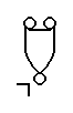
Connected Wires
-
-
Connected wires are drawn in the wire layer
(currently black.) Joined wires are indicated
by placing a connector dot at the junction
of the two wires. Alternaively, if three
wires all end at the same location, HobECAD
assumes that they are connected together.
Some examples are shown below:
-
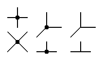
Crossing Wires
-
Wires that cross over one another are
represented by just having straight
lines cross over one another in the
wire layer (currently black.) No
connector dot is present. A couple
of examples are shown below:
-
Labeled Wires
-
Unterminated horizontal or vertical wires
that end in a label are called `labeled
wires'. Labeled wires are how you connect
wires between multiple schematic diagrams.
All wires with the same label are connected
together by HobECAD. By the way, the labels
strings must be in the wire layer (i.e.
black.) labeled wires including overbar labels are
shown below:
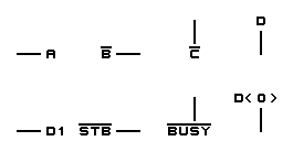
Note that some of the labels in the examples
above have a line drawn over them. These
labels are called `overbar labels'. Overbar
labels are quite common in digital circuits
where they indicate an `active low' signal.
Overbar labels ard drawn using the control-O
`overbar toggle control'. Each time you type
control-O, it will toggle label insertion
between overbar mode or non-overbar mode.
Currently, there is no feedback in the cursor
block to indicate whether or not HobECAD is
in overbar mode or not (this is bug!)
-
Labeled Components
-
It is also possible to insert a component
directly into a schematic. If there is
exactly one label `next' to the component,
the label is taken as component name. The
component lead names are assumed. Some
examples are shown below:
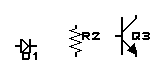
-
Labeled Component Leads
-
It is also possible to insert a component
into a schematic and explicitly label each
of the component leads. The rule is that
HobECAD will find the label closest to each
component lead and use that as the component
lead name. The remaining label that is
`next' to the component is used as the
component name. Some examples are shown
below:
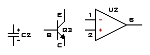
Note that the operational amplifier has a
couple of labels in the annotation layer
(shown in brown). HobECAD completely
ignores labels in the annotation layer.
Thus the component leads for the operational
amplifier are labeled `1', `2', and `6';
the annotation labels of `+' and `-' are
completely ignored.
-
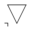
Component Boxes
-
With one exception, all lines and labels
drawn in the annotation layer (i.e. brown
layer) are ignored by HobECAD. The only
exception is a component box. A component
box is a rectangular box drawn in the
annotation layer that encloses a single
black label. The black label is component
name and any black wires that terminate
at the edge of the box must be labeled
in black as component leads. Some example
component boxes are shown below:
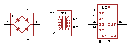
Please note that anything in brown enclosed
in the componet box is ignored by HobECAD.
Further note that for `U3' that there is
a brown `A' afterwards that is ignored by
HobECAD. Finally, note that the wires for
`U3' on the left have wires that are quite
close to one another; HobECAD is smart
enough to figure out which component lead
names are attached to which components
by figuring out whether a vertical sequence
of labels is `on top' or `on bottom'.
The file formats are:
The schematic capture and printed circuit board
formats are the same. They consist of the following
records:
-
H major minor cell_width cell_height cells_wide
cells_high schematic_capture relative_mode
-
This is the first record, where the f
-
major
-
This is the major version number and
is currently version 1.
-
minor
-
This is the minor version number and
is currently version 3.
-
cell_width
-
This is the cell width and currently
must be either 10 or 15 pixels.
Realistically, schematics must be
in cell size 10.
-
cell_height
-
This is the cell height and must
match the cell width.
-
cells_wide
-
This is the number of cells wide the
diagram is.
-
cells_high
-
This is the number of cells high the
diagram is.
-
schematic_capture
-
This is 1 if the diagram is a schematic
and 0 for a printed circuit board.
-
relative_mode
-
This is 1 if the the (x, y) values are
relative format. This is 0 if the (x, y)
values are absolute.
-
I layer x y chunk_label
-
This is a chunk record.
-
S layer x y string
-
This is a string record. The eight bit is turned
on to represent over-bar characters. Any
character that is not a printing ASCII character
is represented as a decimal number enclosed in
back slashes.
-
L layer x1 y1 x2 y2
-
This is the line record.
-
V x y [size [component_name]]
-
In schematic mode, only the x
and y are present. In printed
circuit board mode, the hole size must
be present and the component name may
be present.
-
E
-
This is the last (end) record.
{Font format goes here}
The part list file specifies the parts list for
a printed circuit board and corresponding schematic
files. The file format looks as follows:
    # Comment start with a sharp ('#') character.
    # Blank lines are ignored.
    component_name1: part_name1
    #...
    component_namen: part_namen
A component name consists of one or more letters
(usually capital letters) followed by a decimal
number. Some examples are `U1', `R23', and `LED5'.
The package name comes from some package file
(e.g. `74LS00', `2N2222', etc.) A range of
component names can be specified by adding
a dash (`-') followed by another decimal number,
where the second decimal number is greater
than the first one. Some examples are `R1-R39',
'C40-56',and `U12-14'. The following is
not legal `R12-4' because the second decimal
number (4) is less than the first one (12);
the user probably meant `R12-14'.
Package format specifies the pad locations
for a particular kind of component package
(e.g. TO-220, DIP16, etc.) The suffix of a
package format file must be .pkg.
The contents of a package file is as follows:
    # Comment start with a sharp ('#') character.
    # Blank lines are ignored.   The first non-comment
    # line is the header and must be exactly:
    H Packages 1 0

    P package_name
    L x1 y1 lead_name1 [*]
    #...
    L xn yn lead_namen

    #...

    P package_name
    L x1 y1 lead_name1 [*]
    #...
    L xn yn lead_namen

    # The last line must be and end rerord:
    E
The P record provides the package name
(e.g. `DIP16', `TO-220', etc.) The L records
provide lead information about the package.
The package is oriented so that it points `down'.
For example, a standard DIP (Dual In-line Package)
would be oriented `down' by have pin 1 at the
lower right. In general, the lower left pin
is positioned so that its (x, y) coordinate is
at (0, 0). The (x, y) coordinates are specified
as integer multiples of .05 inch. The lead
names can be an arbitrary sequence of characters
excluding an asterik (`*'). Examples of lead
names are `E', `B', `C', `1', `14', `+', and `-'.
Finally, one of the pins is marked with an asterik
(`*'). This is called the pivot pin. As the
package is reoriented with the less than (`<'),
greater than (`>'), and carret (`^') characters,
the package is rotated around this pin. After
rotation, the package is always translated so
that the lower left corner of the rectangle that
encloses the pads that make up the package are
is at the point specified by the control-P.
Below is a package description for an 8-pin
DIP:
    P DIP8 # 8-pin Dual In-line Package
    L 0 6 5
    L 0 4 6
    L 0 2 7
    L 0 0 8
    L 6 0 1*
    L 6 2 2
    L 6 4 3
    L 6 6 4
Pin 5 is at (x, y) coordinate (0.0", 0.3").
PIn 8 is at (x, y) coordinate (0.0", 0.0").
Pin 1 is at (x, y) coordiante (0.3", 0.0") and
is the pivot lead.
In the future, this format should be made
graphical. It would be easier to describe
and to use. Also, a minimum hole size should
be specified.
Part file format is used to specify the particular
component. The file format is as follows:
    # Comment start with a sharp ('#') character.
    # Blank lines are ignored.   The first non-comment
    # line is the header and must be exactly:
    H Parts 1 0

    P part_name package_name
    L physical_lead_name1 logical_lead_name1 signal_type1
    #...
    L physical_lead_namen logical_lead_namen signal_typen

    #...

    P part_name package_name
    L physical_lead_name1 logical_lead_name1 signal_type1
    #...
    L physical_lead_namen logical_lead_namen signal_typen

    # The last line must be and end rerord:
    E
The P record specfies the part name (e.g. `74LS00',
`2N2222', `1N4001', `NE555', etc.) followed by
a package name (e.g. `DIP14', `TO-220', etc.).
The part name comes from a package file.
The L record specifies the physical package lead
to logical lead name and signal type. The
physical lead name comes from an L record in
the appropaiate package file. The logical
lead name comes from a databook (e.g. `CLK',
`Q1', `Q*', `Emitter', `Collector', etc.)
Finally, the signal type is one of the following:
-
Ground
-
This lead must be connected to ground. The
schematic must show the connection visually.
-
Ground_Implied
-
This lead must be connected to ground. The
schematic does not visually show the
connection.
-
No_Connection
-
Nothing should be connected to the lead.
-
Other
-
This lead has some kind of non-digial signal
on it. An Other lead can be connected to
any other lead without complain from the
HobECAD checker.
-
Pull_Down
-
This lead is one end of a pull down resistor.
The other end is connected to Ground.
-
Pull_Up
-
This lead is one end of a pull up resistor.
The other end is connected to Vcc. This
lead can safely be connected to a TTL
Open Collector lead.
-
TTL_In
-
This lead is a TTL (Transistor-Transistor
Logic) input lead. It can be connected to
either a TTL_Out lead or a TTL_Open_Collector
lead (and a corresponding Pull_Up lead.)
-
TTL_Open_Collector
-
This is a TTL Open Collector output lead.
It needs to be connected to a Pull_Up lead.
It can safely be connected to a TTL_In lead.
-
TTL_Out
-
This is a TTL Output lead. It can be
connected to at TTL_In lead..
-
TTL_Tristate
-
This is a TTL Tristate lead. It can be
connected to a TTL_Tristate lead.
-
Vcc
-
This is the common supply voltage. This
connection must be explicitly shown in
the schematic.
-
Vcc_Implied
-
This is the common supply voltage. This
connection is not to be shown in the
schematic.
Other signal types will be added as needed.
As with the package format, this file should be
converted to a graphical format.
With the growing proliferation of surface mount
components, the fundamental design choice of
putting all components on a .05 inch grid is
becoming suspect. However, as of the late 1990's,
HobECAD still meets my goal of being a
schematic capture and layout program for
electonics hobbiests. Professional electrical
engineers should purchase and utilize full
featured schematic capture and layout products.
Copyright (c) 1995, 1998, 2000 by
Wayne Gramlich All rights reserved.