This is one of my CNC motion control revisions and it is currently an abandoned project.
This is the Revision A version of my motion control board. I took this design pretty much to the completion of the printed circuit board layout. Unfortunately, I ultimately decided that I had partitioned things incorrectly and have wound up designing a significantly different board called Revision B (original name!) You should only be digging around in this design if you enjoy seeing circuit board evolution.
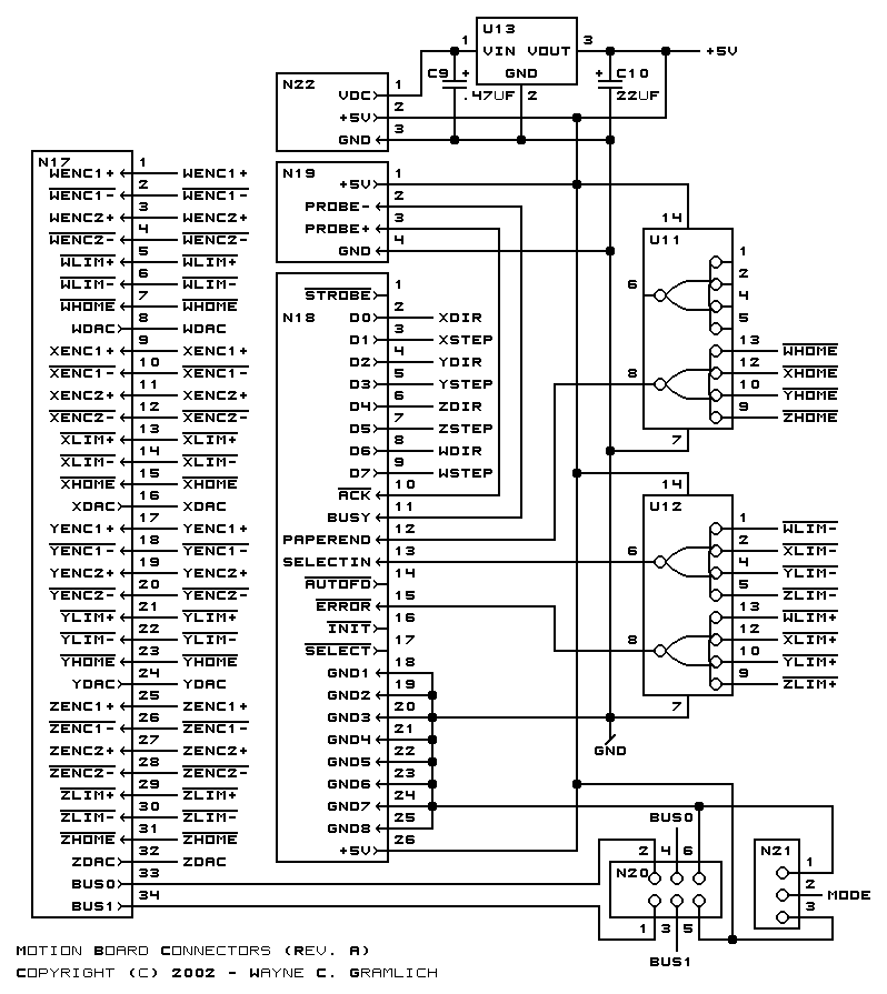
There is an additional connector that is only used when the motion board is connected to the buffer board. This connector is used to collect the linear/shaft encoder signals, the individual limit/home switch signals, control the wave tables, and control the Digital to Analog converters (discussed a litte further below.) The buffer connector is a standard ribbon cable with the following pinouts:
Pin Number Label Direction 1 WENC1+ Out 2 WENC1- Out 3 WENC2+ Out 4 WENC2- Out 5 WLIM+ Out 6 WLIM- Out 7 WHOME Out 8 WDAC In 9 XENC+ Out 10 XENC1- Out 11 XENC2+ Out 12 XENC2- Out 13 XLIM+ Out 14 XLIM- Out 15 XHOME Out 16 XDAC In 17 YENC1+ Out 18 YENC1- Out 19 YENC2+ Out 20 YENC2- Out 21 YLIM+ Out 22 YLIM- Out 23 YHOME Out 24 YDAC In 25 ZENC1+ Out 26 ZENC1- Out 27 ZENC2+ Out 28 ZPhase2- Out 29 ZLIM+ Out 30 ZLIM- Out 31 ZHOME Out 32 ZDAC Out 33 Bus0 In 34 Bus1 In
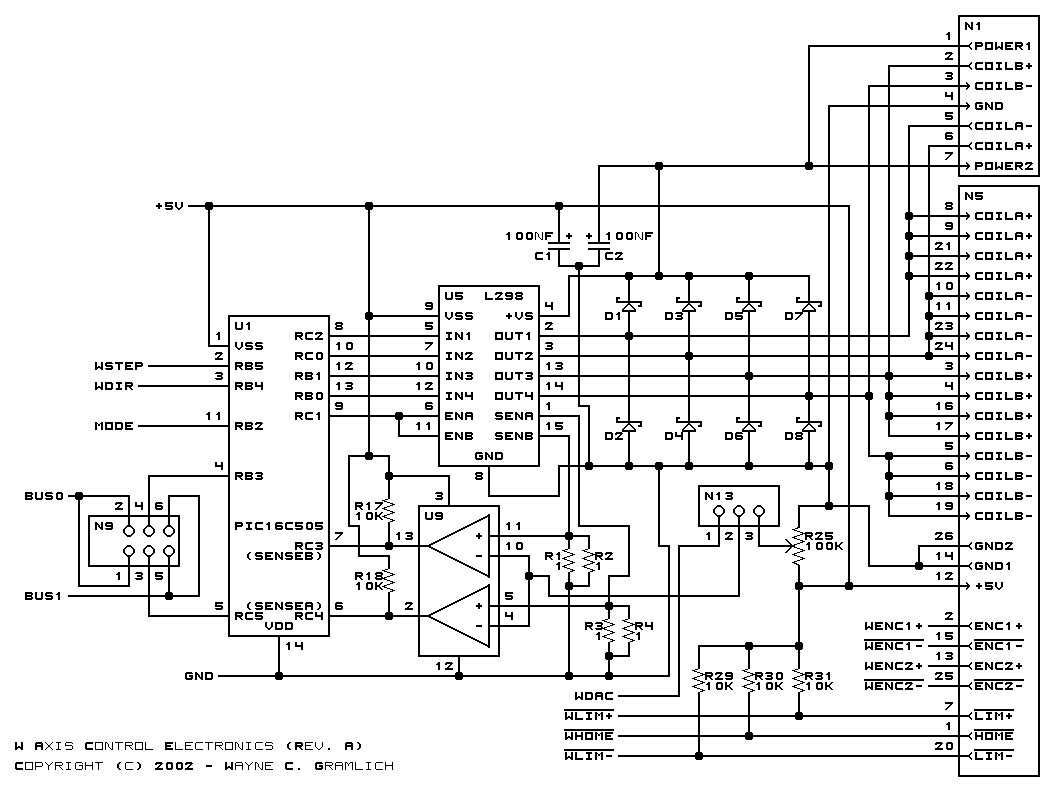
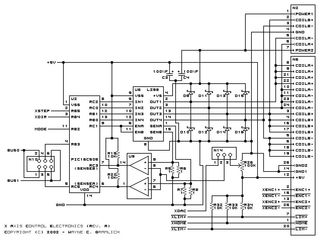
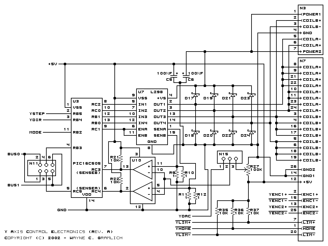
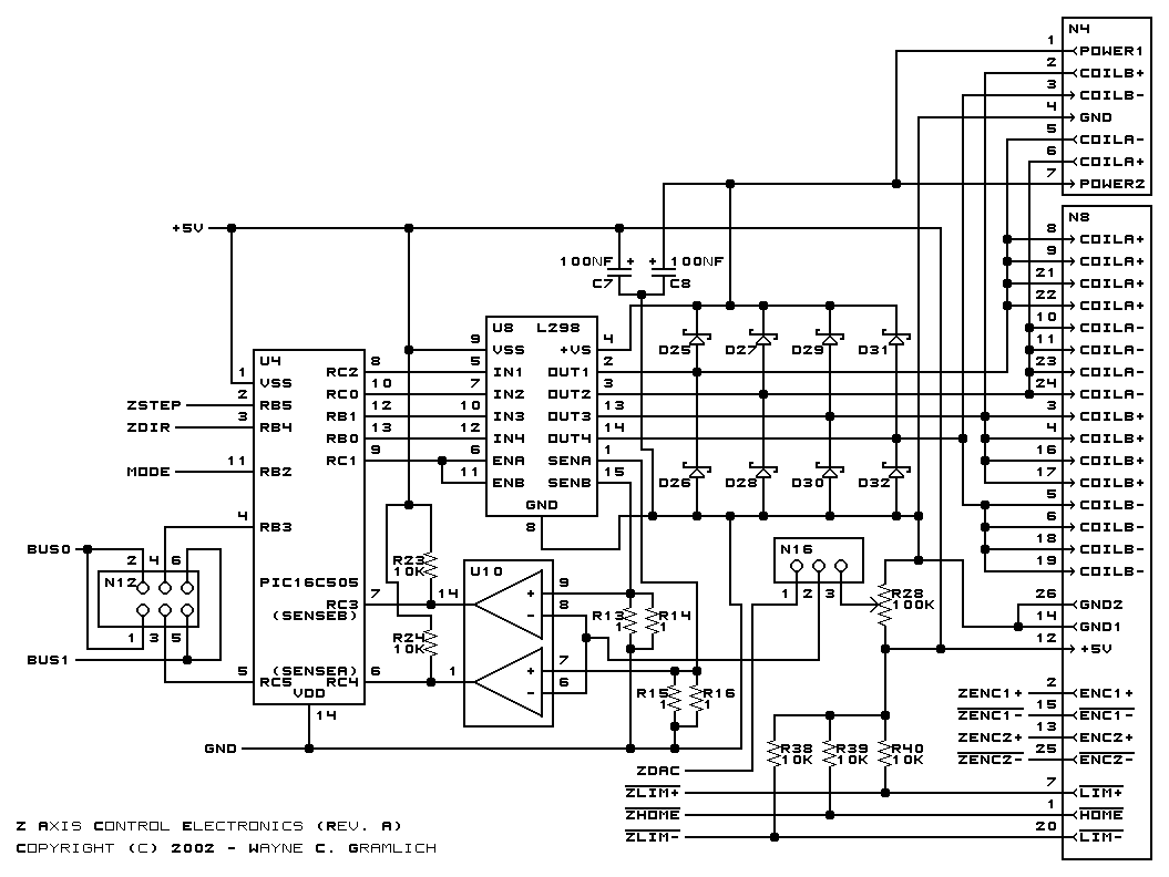
My preference is to use a less expensive Microchip PIC16C505 [PIC16C505] instead of a L297. This 14-pin chip in conjunction with a simple comparator chip can perform basically the same functions as the L297.
The PIC16505 has a drawback in that it needs to be programmed. This is solved by providing a very simple serial programming circuit as part of the motion board electronics. (I never actually got around to putting this on the board.)
There are 12 I/O pins on PIC16C505:
The STEP, DIR, MODE, BUS0, and BUS1 lines are used to control the PIC16C505. When MODE=0, the PIC16C505 is in stand-alone mode and the wave tables are selected by applying a 1 or 0 to BUS0 and BUS1 respectively. When MODE=1, the BUS0 and BUS1 lines of all othe PIC16C505's are tied together. By setting the DIR, BUS0, and BUS1 lines, the buffer board can remotely configure the PIC16C505.
Pin Function Number Label 13 RB0 STEP 12 RB1 DIR 11 RB2 MODE 4 RB3 BUS0 3 RB4 BUS1 2 RB5 ENABLEAB 10 RC0 COILA+ 9 RC1 COILA- 8 RC2 COILB+ 7 RC3 COILB- 6 RC4 SENSEA 5 RC5 SENSEB
MODE STEP BUS0 BUS1 DIR Description 0 0->1 x x 0 Step Clockwise 0 0->1 x x 1 Step Counter Clockwise 0 x 0 0 x Wave Table 0 0 x 0 1 x Wave Table 1 0 x 1 0 x Wave Table 2 0 x 1 1 x (Reserved) 1 0->1 0 0 0 Step Clockwise 1 0->1 0 0 1 Step Counter Clockwise 1 0->1 0 1 0 Disable 1 0->1 0 1 1 Enable 1 0->1 1 0 0 Increment Delay 1 0->1 1 0 1 pDecrement Delay 1 0->1 1 1 0 Increment Wave Table 1 0->1 1 1 1 Reset
The schematics are broken into 1 connectors schematic and 4 relatively identical axis schematics.
The parts list is kept in a separate file.
The connectors schematic is shown below:
The W Axis schematic is shown below:
The X Axis schematic is shown below:
The Y Axis schematic is shown below:
The Z Axis schematic is shown below:
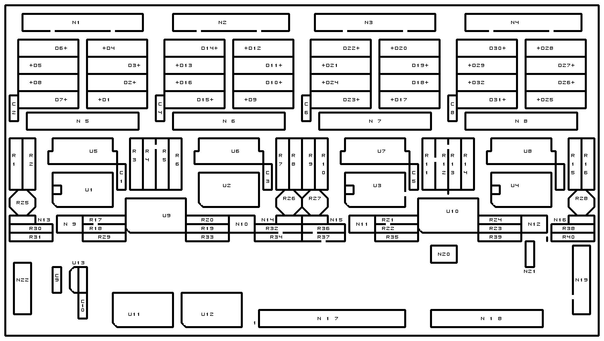
The printed circuit board files are listed below:
There are a number of problems with the Revision A board: