This is the revision A version of the IO8 module.
The IO8 module connects provides 8 selectable input/output pins. The pins can be digital input, digial output, or analog input. The analog input pins can measure up to 10 bits resolution between 0 and 5 volts.
Command
NameBit Action Description 8 7 6 5 4 3 2 1 0 Digital8_Read 0 0 0 0 0 0 0 0 0 Send Return the digital input values for all 8 pins dddd dddd 0 d d d d d d d d Receive Digital8_Write 0 0 0 0 0 0 0 0 1 Send Write oooo oooo to the 8 digital outputs. iiii iiii is the 8 digital inputs before the write and dddd dddd is the 8 digital inputs after the write. 0 i i i i i i i i Receive 0 o o o o o o o o Send 0 d d d d d d d d Receive Direction_Read 0 0 0 0 0 0 0 1 0 Send Return the digital direction mask dddd dddd (0=output, 1=input). 0 d d d d d d d d Receive Direction_Set 0 0 0 0 0 0 0 1 1 Send Set the direction mask to dddd dddd (0=output, 1=input). 0 0 0 0 0 0 0 0 0 Receive 0 d d d d d d d d Send 0 0 0 0 0 0 0 0 0 Receive Analog_Read 0 0 0 0 0 0 1 0 0 Send Return the analog mask aaaa aaaa (0=digital, 1=analog). 0 a a a a a a a a Receive Analog_Set 0 0 0 0 0 0 1 0 1 Send Set the analog mask to aaaa aaaa (0=digital, 1=analog). 0 0 0 0 0 0 0 0 0 Receive 0 a a a a a a a a Send 0 0 0 0 0 0 0 0 0 Receive Analog8_Read 0 0 0 0 1 0 c c c Send Return the 8-bit analog input for channel ccc as aaaa aaaa 0 a a a a a a a a Receive Analog10_Read 0 0 0 0 1 1 c c c Send Return the 10-bit analog input for channel ccc as aaaa aaaa bb. 0 a a a a a a a a Receive 0 0 0 0 0 0 0 0 0 Send 0 b b 0 0 0 0 0 0 Receive Low_Set 0 0 0 1 0 d d d d Send Set the low 4 bits of the digital outputs to dddd. The 8-input bits iiii iiii are read after setting. 0 i i i i i i i i Receive High_Set 0 0 0 1 1 d d d d Send Set the high 4 bits of the digital outputs to dddd. The 8-input bits iiii iiii are read after setting. 0 i i i i i i i i Receive Common
Commands0 1 1 1 1 1 1 x x Send Standard common command. See specifications for details. 0 a a a a a a a a Receive Select 1 a a a a a a a a Send Select the module with an address of aaaa aaaa. A time-out indicates that the module is not selected. 0 0 0 0 0 0 0 0 0 Receive
The hardware consists of a circuit schematic and a printed circuit board.
The parts list kept in a separate file -- io8.ptl.
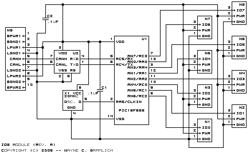
The schematic for the IO8 module is shown below:
The bus is connected to the 2×5 shrouded conenctor N9. The two CAN bus signals are fed into the PCP2551 CAN bus transceiver U2. The output of U2 is fed to the UART transmit and receive signals on the PIC16F688 microcontroller U1. 8-pins of the U1 are connected to 1×3; polarized .1" male headers. Each pin is connected to one of the anlog inputs on U1. A half size crystal oscillator (X1) is used to provide the reference 20MHz signal. A resonator could not be used since it requires pins 2 and 3 of U1, and pin 3 is needed for a analog input (AN3).
The printed circuit board files are listed below:
The following files are available:
The following fabrication issues came up: