This is revision A of my cheap PIC programmer project.
The revision B printed circuit board has not been sent out for fabrication yet. It corrects a number of problems were encountered and documented in the Revision A Notes section.
Ultimately, I was unable to get the revision A circuit to work with the tri-state buffers (even when I used a 74HC125.) When I looked around the net, everybody was using open collector technology instead of tri-state technology. So, I switched over to open collector and it all started to work.
The revision B schematic is shown below:
The circuit works as follows.
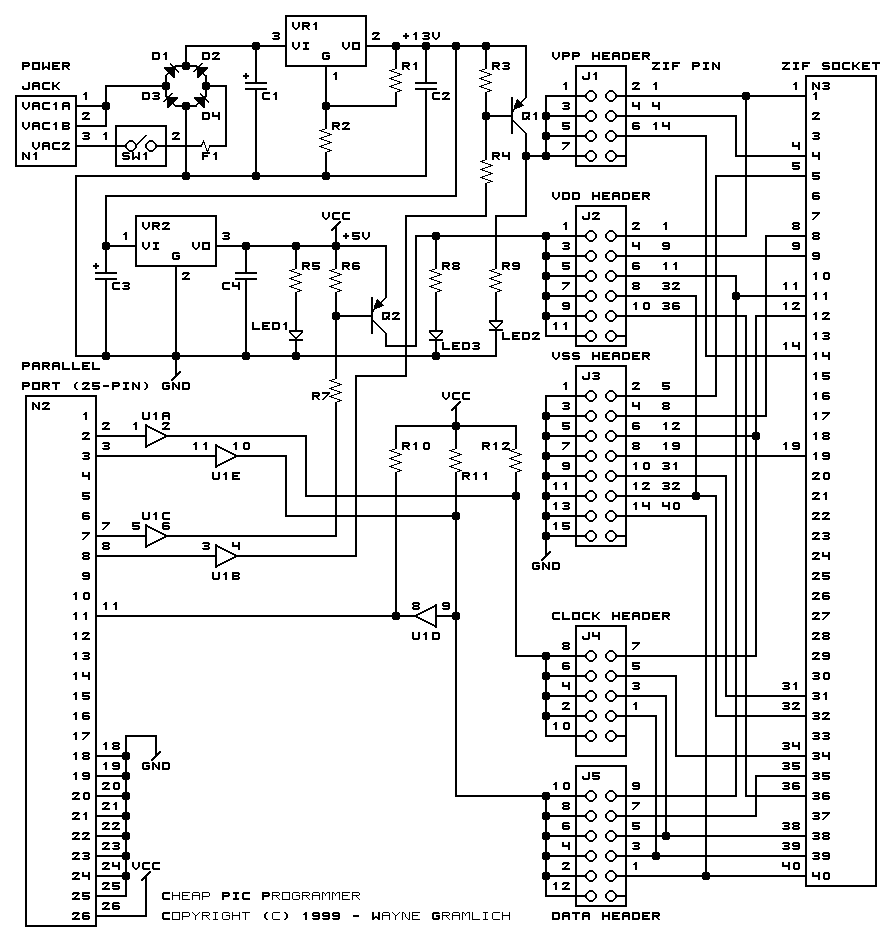
A wall wart transformer provides 24VAC through power jack N1. The 24VAC goes through a power switch SW1, Fuse F1, and full wave diode rectifying bridge made of diodes D1 through D4. An electroylitic capacitor, C1, a variable voltage regulator, VR1, and a tantalum capacitor, C2, provide a 13 volt linear power supply. The output voltage of 13 volts is set by appropriate selection of resistor values R1 and R2. Please note that VR1 runs quite hot, so a heat sink is required. The electrolytic capacitor, C3, 5 volt voltage regulator, VR2 and tantalum capactior, C4, provide a 5 volt power supply. Resistor R5 and LED1 provide a power on indicator.
Signals from the controlling computer's parallel port interface come in on connector N2. The clock signal comes in on N2 pin 2 (DATA1) and is buffered by U1A and pull-up R12. The data comes in on N2 pin 3 (DATA2) and is buffered by U1E and pull-up R11. Pin 7 (DATA6) and pin 8 (DATA7) are used respectively to control the application of Vss and Vpp to the chip. The Vpp control comes in on N2 pin 8 (DATA7) and is buffered by U1B. R3, R4, and Q1 form a 13 volt voltage follower that is enabled when U1B pin 4 goes low. Resistor R9 and LED2 provide an indicator of when Vpp is enabled. The Vdd control comes in on N2 pin 7 (DATA6) and is buffered by U1C. R7, R6, and Q2 form a 5 volt voltage follower that is enabled when U1C pin 6 goes low. Resistor R8 and LED3 indicate when Vdd power is applied.
Headers J1, J2, J3, J4, and J5 are used to route Vpp, Vdd, Vss, Clock and Data signals to the 40-pin ZIF chip N3. A shorting block is applied to each header to route the correct signal and voltage to the chip being programmed.
The revision A PIC programmer printed circuit board has been layed out. The following files are available:
As I build each project, I type notes to myself immediately below. I consult these notes whenever I do another revision of the board:
http://www.blichfeldt.dk/Namely jumper elimination and production quality programming.