This is revision A of my
cheap PIC programmer project.
Cheap PIC Programmer (Revision A)
The revision A printed circuit board was sent out
for fabrication in mid-February 1999. A number of
problems were encountered and documented in the
Notes section below.
The revision A schematic is shown below:
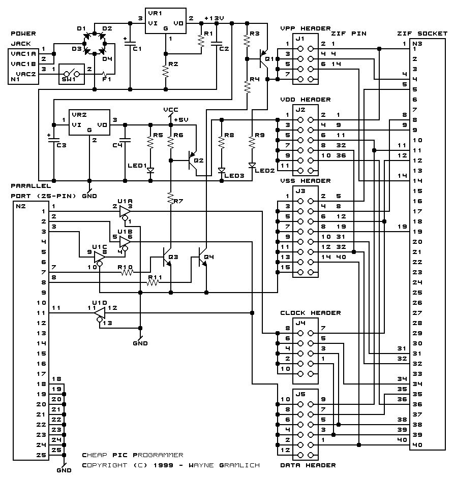
The circuit works as follows.
A wall wart transformer provides 24VAC through power
jack N1. The 24VAC goes through a power switch SW1,
Fuse F1, and full wave diode rectifying bridge made
of diodes D1 through D4. An electroylitic capacitor,
C1, a variable voltage regulator, VR1, and a tantalum
capacitor, C2, provide a 13 volt linear power supply.
The output voltage of 13 volts is set by appropriate
selection of resistor values R1 and R2. Please note
that VR1 runs quite hot, so a heat sink is required.
The electrolytic capacitor, C3, 5 volt voltage
regulator, VR2 and tantalum capactior, C4, provide
a 5 volt power supply. Resistor R5 and LED1 provide
a power on indicator.
Signals from the controlling computer's parallel
port interface come in on connector N2. The
clock signal comes in on pin 1 (STROBE). The
data comes in on pin 2 (DATA1). Pin 3 (DATA2)
is used to control the tri-state output of buffer
U1B. Pin 7 (DATA6) and pin 8 (DATA7) are used
respectively control the application of Vss
and Vpp to the chip. Resistor R10, transistor
Q3, resistor R7, resistor R6 and transistor
Q2 provide a 5 volt voltage follower. Resistor
R8 and LED1 indicate when Vdd power is applied.
Similarly, resistor R11, transistor Q4,
resistor R4, resistor R3 and transistor Q1
provide a voltage follower for Vpp. Resistor R9
and LED2 indicate when Vpp power is applied.
Headers J1, J2, J3, J4, and J5 are used to route
Vpp, Vdd, Vss, Clock and Data signals to the
40-pin ZIF chip N3. A shorting block is applied
to each header to route the correct signal and
voltage to the chip being programmed.
The revision A PIC programmer printed circuit board
has been layed out. The following files are available:
-
PIC Programmer PCB Artwork Layer
-
This contains the artwork layer that specifies
where the components are to be placed.
-
PIC Programmer PCB Back Layer
-
This is the back (solder) side of the board.
-
PIC Programmer PCB Front Layer
-
This is the front (component) side of the board.
-
PIC Programmer PCB Excellon Drill File
-
This is the drill file for the PCB in industry
standard Excellon format.
-
PIC Programmer PCB RS-274X Back Layer
-
This is the industry standard RS-274X file
that specifies the apertures and line placement
for the back layer.
-
PIC Programmer PCB RS-274X Front Layer
-
This is the industry standard RS-274X file
that specifies the apertures and line placement
for the front layer.
-
PIC Programmer PCB Drill Size File
-
This is a short file that specifies the drill
sizes for the Excellon drill file.
-
PIC Programmer PCB Parts List File
-
This is a the parts list file.
-
PIC Programmer PCB Size and Hole Counts
-
This is a short file that specifies the board
size and hole count.
As I build each project, I type notes to myself
immediately below. I consult these notes whenever
I do another revision of the board:
-
Move the power jack up .1 inch.
-
The holes for the power jack cause problems at
Alberta Printed Circuits.
HobECAD needs to be tweaked to provide better
handling of large holes.
-
The diode holes for D1-D4 need to be enlarged
by one.
-
Move the capacitors over by one so that the
heat sink will `cup' them.
-
The LED's are too close to the ZIF socket.
They are also too close together.
-
The emitter and collector on Q1 and Q3 are swapped.
The base is just fine.
-
The artwork on the PN2222's is upside down.
-
The copper letters "CLK" and "DATA" are
swapped.
-
The PIC16F8x needs to run CLK to pin 34.
The copper lettering (on the mislabeled
CLK header) says pin 35 rather than pin 34.
The lettering is incorrect, it really does
run to pin 34.
-
There should be a 5V connection to pin 26
of the parallel port to provide power to
my parallel port simulator.
-
The schematic should have little circles on
the inputs to the 74LS125 bus drivers.
Alternatively, switch over to a 74LS126
and tie the inputs to Vcc. Actually, I
should use a 7407 instead.
-
Pin 1 of the parallel port connector should
be made visible in copper lettering.
-
There is some room between the power jumpers
and the 40-pin connector that could be squeezed
out.
-
Think about moving the pins around to match
another programmer so that people can use
that programmer's software.
-
Consider using a 10-turn pot to set the
program voltage.
-
Run everything off of the data pins. It is
difficult to control the Clock pin sometimes.
-
Consider little boards with resisters and LED's
that emulate the more common PIC's.
Copyright (c) 1999 by
Wayne Gramlich. All rights reserved.