This is part of the MRNet project.
A wired cab station provides the electronics for adapting MRNet signals from their RJ45 RS-422 signals to a 3-wire wired cab cable that connects a wired cab to the wired cab station. Multiple different wired cabs can connect to this station as long as they obey the 3-wire power and signal conventions.
This wired cab station module is designed around the MAX232A dual RS-232 receiver/driver chip from Maxim and the 26LS132 quad RS-422 line receiver available from mulitple vendors. An important consideration is make sure that unused connectors do not `jam' the bus. Thus, it is important to understand what signal is output form each of these chips in the `open' state.
For the MAX232, the output state is summarized in the table below:
A further tid-bit of information is that an `idle' RS-232 serial connection is at -10 volts.
Input Output Open H < .8 volts H > 2.4 volts L
The 26LS132 takes a differential RS-422 signal as input and produces a TTL output signal. The following table is copied out of the data sheet for the Texas Instruments version of the part:
Differntial A-B G G* Output Y Positive H X H Positive X L H Negative H X L Negative X L L Open H X H Open X L H X L H Z
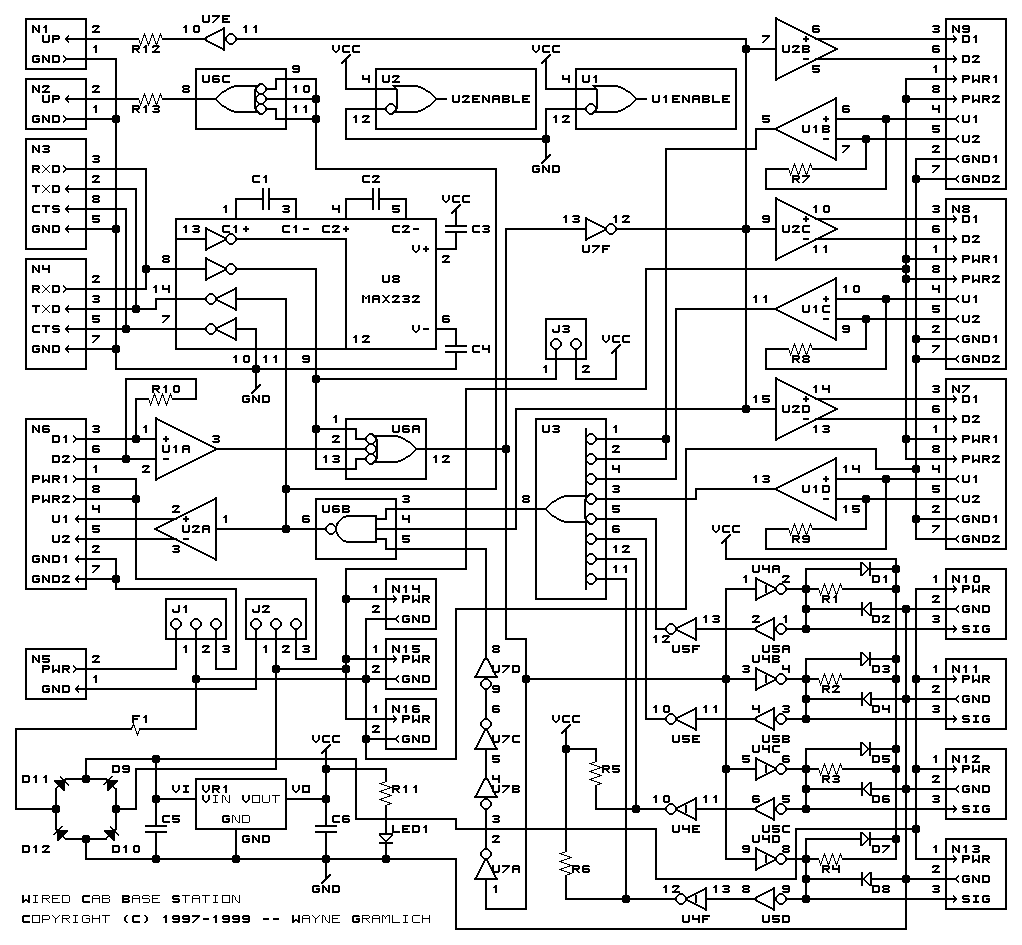
The schematic for the cab station is immediately below:
Power and ground come in on connector N5 for the `root hub'. The non-root boards get their power and ground via the RJ45 connector N6. In all cases the power and ground are sent off to the other boards via the RJ45 connectors N7-N9. The handheld cabs get their power from phone jacks N10-N12. The power coming in needs to be at least 6.5 volts so that it can be regulated by VR1, C5, and C6 into 5 volts. R11 and LED1 provide a `power on' indicator.
If the board is being used as a `root hub', a MAX232 is installed on the board as U8 along with the capcitors C1-C4 to perform the RS-232D to TTL level conversion. Capacitors C1-C4are used by the MAX232 charge pumps to provide the +/- 10 volts needed for the RS-232D voltage levels. An `idle' serial connection is at -10 volts. The RS-232 signal comes in on either the 9-pin RS-232D connector N3 or the 25-pin RS-232D. Both `idle' and `open' produce the same output high signal on U8 pin 9. Switching over to the uplink signal, which comes from U6B pin 6, this is run straight through to U8 pin 11 and out to the transmit pings of connectors N3 and N4. Finally, the pin 10 of the U8 is grounded to generate a +10 volt CTS (Clear To Send) signal back through N3 and N4. Any boards that are being used in a non `root hub' fashion, can skip the installiation of the MAX232 and associated capacitors C1-C4. That pretty much covers the RS-232D portion of the circuit.
In all non `root hub' boards, the down link signal comes in through RJ45 connector N6 into the differential RS-422 receiver inputs of U1A. R10 is a line termination resistor that matches the characteristic impedance of the line. In order to prevent a `jam', both an `open' and `idle' signal on U1A produce a `high'. When a signal is present on the down link, pin 3 of U1A goes low. U6A OR's the down link signal from N6 and U1A with the down link signal from the RS-232 connectors N3/N4 and U8. Only one down link signal is ever expected to be present. The output of U6A pin 12 goes to inverter U7F pin 13 where it is inverted and distributed to the RS-422 drivers U2B, U2C, and U2D and the signals are output on RJ45 connectors N7-N9. The down link signal is inverted yet once more via inverter U7E which is connected to connector N1 via resistor R12. A simple LED is connected to N1 to show downlink activity. Finally, U2 is forced to always be enabled by grounding pin 12 and connecting pin 4 to Vcc. That pretty much covers the down link portion of the circuit.
Up to 4 handheld cabs can be connected to the board via 3 wire phone jacks N10 through N13. Power and ground are connected to two of the phone jacks connectors. The remaining connector forms a bi-directional open-collector bus with the handheld cab. The down-link signal comes from U6A pin 12 and gets inverted by open collector inverters U4A, U4B, U4C, and U4D. Resistors R1-R4 are the pull up resistors for the shared bus. Dioded D1-D8 are clamping diodes to protect from voltage spikes when the handheld cabs are plugged into the phone jacks N10-N13.
When the handheld cab wants to send an up link signal, it waits for its turn. When the down link is idle, it transmits is information on the open collector bus (active low.) The signal is inverted via schmidt trigger inverters U5A, U5B, U5C, and U5D. The up link signal is reinverted by inverters U5E, U5F, U4E, and U4F. Since U4 is an open collector inverter, resistors R5 and R6 are used to pull their outputs high. All of these up-link signals go into the 8-input NAND gate U3 where they are OR'ed together with the up link signals from RS-422 receivers U1B, U1C, and U1D connected to the RJ45 connectors N7-N9. Resistors R7-R9 are impedance matching resistors to match the characteristic impedance of the RS-422 line. Again, both `idle' and `open' connections to N7-N8 produce no `jam' signal.
The 3-input NAND U6B needs a bit of discussion. U6B in conjunction with the inverters U7A, U7B, U7C, and U7D provide an `echo supression' circuit. When a down-link signal comes down from N3, N4, or N6, it ultimately causes the signal lines on phone jacks N10-N13 to be asserted `low'. These signals are immediately fed back up to the up-link circuit. If all of the boards on the tree did this, the resulting `hash' on the up-link would be pretty ugly, since each board would have a slightly different delay. To eliminate the `hash', an echo supressor is used. Whenever a down link signal is present, it immediately disables the up link signal at U6B pin 4. When the up-link signal is removed, it will take a short while for the signal to propagate through to U3. The delay line formed by inverters U7A, U7B, U7C, and U7D `stretch' the down-link signal to keep the up link signal disable via U6B pin 5. That pretty much wraps up the entire circuit.
The printed circuit board for the wired cab station has been layed out. The following files are available: