This is the A revision of the EMDP1 Bootstrap Adaptor. It is a work in progress.
The bootstrap adaptor is used to download a boot loader into the PIC16F877 in the EMDP1 for the first time. After the boot load is installed, additional EMDP1 firmware updates can be installed via the boot loader. In theory, the bootstrap adaptor only needs to be used once.
The bootstrap adaptor requires either a serial RS-232 connection to the host computer. While both serial and parallel port connections are standard on the older mother boards based on the Intel x86 processor architecture, the newer mother boards are tending to use USB instead. If you are using one of the newer mother boards, you will have to purchase a USB to serial adpator to talk to the EMDP1. (Maybe the EMDP2, will have a USB connector instead of a serial connector.)
Some specialized software is needed to download the boot loader via the bootstrap adaptor.
By way of review, the RS-232 standard represents a zero with a voltage between 3 and 15 volts and a one with a voltage between -3 and -15 volts. The popular MAX232 chip converts from RS232 levels to 5 volt logic levels. For, serial communications, RS232 idles at one (i.e. a negative voltage.) When a byte is sent, there is a start bit at logic low, followed by 8 bits of data, starting with the least significant bit (LSB) to the most significant bit (MSB), followed by a single high start bit. This is called 8N1 (8 data bits, No parity, 1 stop bit) format.
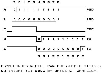
For example, the letter `+' has a decimal code of 43 (octal 53, hex 2b, binary 00100011). The waveform for code 43 looks as shown below:
Please note that even though the line idles at high, the data is not inverted. A zero in the code is sent using a zero logic level and vice versa.
The circuit below is designed around a series of one-shot multivibrators (one-shot for short.) In order to simplify things, the bootstrap adaptor only uses characters that can be represented using a single square waveform that transitions from an idle at 1, down to 0, and back up to idle at 1 again. There are exactly eight codes that have this property and they are represented in the table below:
Code Transmit Sequence
(Left to Right)Pulse Length
(bits)Decimal Binary 255 11111111 1 254 11111110 2 252 11111100 3 248 11111000 4 240 11110000 5 224 11111111 6 192 11000000 7 128 10000000 8 0 00000000 9
There are three operations that the bootstrap adaptor needs to perform:
The way the circuit below is designed, the host processor sends a command character, and the bootstrap adaptor always responds with a character. Conceptually, there are 4 codes:
The code sequences look as follows:
Notice how the S1 command is used for both sending a 1 and reading a bit back. The host software and PIC together know which `direction' the data is supposed to flow during the programming process. So when it is time to read a bit, the S1 command is sent, and the appropriate bit value is read back from the PIC and sent back as response code R0 or R1 as appropriate.
Send Receive Description S0 R0 Send a 0 S1 R1 Send a 1 S1 R0 Read a 0 S1 R1 Read a 1
The secret decoder table for the codes is:
The reason why both R1 and R0 have three possible response codes is because the resistor and capacitor component values used for the one-shots have +/-5% and +/-10% variance respectively; thus, they can be a little sloppy on the width of the pulse they send back. More precise (and expensive) components could be specified, but they really are not necessary, just so long as the host software interprets the response code appropriately.
Symbol Code(s) S0 255 (= 11111111 binary) S1 0 (= 00000000 binary) R0 255, 254, 252, 248 (= 11111xxx binary) R1 0, 128, 192, 224 (= 00000xxx binary)
The RX signal is fed directly to PGD through an open collector invertor. By sending a 0, the data line on the PIC will see a short blip towards zero, followed by the line remaining at high; this corresponds to 'send a 1' (see B below.) By sending a 255, the data line on the PIC will a signal that is low; this corresponds to a `send a 0' (see A below).
The schematic for the bootstrap adaptor is shown below:
The RX signal comes from the MAX232 RS232 level converter on the EMDP1 via pin 7 on N1. The host computer will transmit either a code S0 (see A below) or a code S1 (see B below). The RX signal is fed straight through open collector inverter U1B to PGD and to pin 1 of U2A. Since pins 2 and 3 of U2A are tied high, a falling edge on RX indicates that a start bit is coming in and triggers one-shot U2A to emit a pulse that is approximately 5 bits long (see C below) The output of Q* on U2A is fed through inverter U1A to PGC. Thus, the output of U2A is the serial clock pulse for the PIC. If a code S0 is received, the RX signal will still be 1, and PGD will still be 0 (because of inverter U2A) when the falling edge of PGC clocks the 0 into the PIC. Similarly, if code S1 is received, the RX signal will still be 0, and PGD will be 1 (because of inverter U2A) when the falling edge of PGC clock clocks the 1 into the PIC.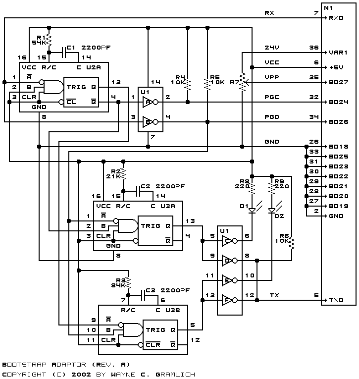
Now it is time to talk about reading out a bit from the PIC. The edge of U2A is fed to either U3A pin 2 or U3B pin 9. The PGD pin is fed directly into the opposite pin on either U3A pin 1 or pin 10 U3B. Thus, the falling edge will trigger U3A to emit a code R0 or U3B to emit a code R1 depending upon whether PGD is a 0 or 1 respectively. The output of U3A and U3B are wired OR'd together via open collector inverters U1D and U1F and sent back to the MAX RS232 level converter on the EMDP1 via pin 5 of N1.
The rules for the 74LS123 are:
T = K×R×Cwhere
R = (N×W) / (K×C)The resistor values for R1-3 are listed below:
= (N×8680) / (.37*2200)
= N×10.663
Ideally, we would choose N=1 for U3A and N=9 for U3B, but because the resistors have +/-5% variance and capacitors have +/-10% variance, we want to have a little room for slop. Hence, N=2 for U3A and N=8 for U3B.
One-shot N R U2A 5 53.4K (R1) U3A 2 21.4K (R2) U3B 8 85.3K (R3)
The following printed circuit board files are avaiable:
Any fabrication issues will be listed here.