This is revision A of the AVR Adaptor Board and it is currently a work in progress.
There is a PDF version of this file available.
The AVR Adaptor Board is used to program Atmel® AVR microcontrollers. Most chips are programmed serially. The ATtiny28 is programmed using a parallel mode.
In order to serially program an AVR one of two serial programming methods is used. The SPI programming method is entered by applying 0 volts to RESET* and talking to the chip using the SPI protocol. The AVR serial programming method is entered by applying 12 volts to RESET*.
This adaptor board directly supports the AVR microcontrollers that are in 8, 20, 28, and 40 pin DIP (Dual Inline Package) packages. Any surface mount AVR microcontrollers will need an alternative adaptor; since I am perfectly happy to use DIP packaging for all of my projects that use AVR microcontrollers, I am in no particular hurry to design an adaptor for surface mount AVR chips.
My going in design decision was that there was going to be a single 40-pin ZIF (Zero Insertion Force) socket and that I would always place pin 1 of each AVR microcontroller in the upper left corner of that socket, irrespective of whether the chip is in an 8, 14, 18, 28, or 40 pin DIP package. The investigation of how this all works is done up on the index.html.
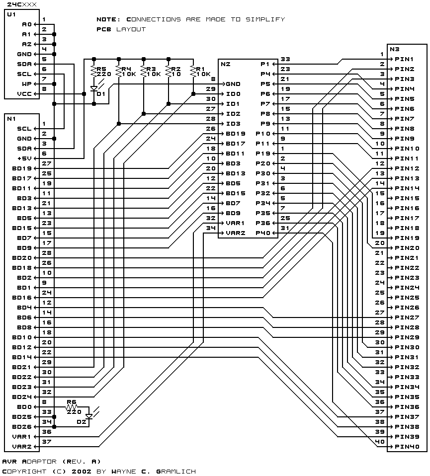
The schematic for the AVR Serial Adaptor is shown below:
The parts list is kept in a separate file.
The various printed circuit board files are listed below:
The EMDP1 connector is listed below:
Pin Label Connected To 1 SCL Serial EEPROM 2 GND Plug Pin 8 3 SDA Serial EEPROM 4 5 6 +5V Serial EEPROM & pull ups 7 8 BD0 Program LED 9 BD1 ZIF40 Pin 13 10 BD2 ZIF40 Pin 12 11 BD3 Plug Pin 10 12 BD4 ZIF40 Pin 27 13 BD5 Plug Pin 12 14 BD6 ZIF40 Pin 28 15 BD7 Plug Pin 14 16 BD8 ZIF40 Pin 29 17 BD9 Plug Pin 16 18 BD10 ZIF40 Pin 37 19 BD11 Plug Pin 18 20 BD12 ZIF40 PIn 38 21 BD13 Plug Pin 20 22 BD14 ZIF40 PIn 39 23 BD15 Plug Pin 22 24 BD16 ZIF40 Pin 14 25 BD17 Plug Pin 24 26 BD18 ZIF40 Pin 3 27 BD19 Plug Pin 26 28 BD20 ZIF40 Pin 2 29 BD21 Plug Pin 28 (ID3) 30 BD22 Plug Pin 27 (ID2) 31 BD23 Plug Pin 30 (ID1) 32 BD24 Plug Pin 29 (ID0) 33 BD25 Ground 34 BD26 Ground 35 BD27 36 VAR1 Plug Pin 32 37 VAR2 Plug Pin 34 38 39 40
Pin Label Connected To 1 P19 ZIF40 Pin 19 2 P20 ZIF40 Pin 20 3 P31 ZIF40 Pin 31 4 P30 ZIF40 Pin 30 5 P34 ZIF40 Pin 34 6 P32 ZIF40 Pin 32 7 P35 ZIF40 Pin 35 8 GND Ground 9 P11 ZIF40 Pin 11 10 BD3 N1 Pin 11 11 P10 ZIF40 Pin 10 12 BD5 N1 Pin 13 13 P9 ZIF40 Pin 13 14 BD7 N1 Pin 15 15 P8 ZIF40 Pin 8 16 BD9 N1 Pin 17 17 P7 ZIF40 Pin 7 18 BD11 N1 Pin 26 19 P6 ZIF40 Pin 6 20 BD13 N1 Pin 21 21 P5 ZIF40 Pin 5 22 BD15 N1 Pin 23 23 P4 ZIF40 Pin 4 24 BD17 N1 Pin 25 25 P36 ZIF40 Pin 36 26 BD19 N1 Pin 27 27 ID2 N1 Pin 30 (BD22) 28 ID3 N1 Pin 29 (BD21) 29 ID0 N1 Pin 32 (BD24) 30 ID1 N1 Pin 31 (BD24) 31 P40 ZIF40 Pin 40 32 VAR1 N1 Pin 36 (VAR1) 33 P1 ZIF40 Pin 1 34 VAR2 N1 Pin 37 (VAR2)
Any fabrication issues will be listed here.