This is one of my CNC motion control revisions and it is currently an work in progress.
This is the Revision C version of my motion control board.
I ultimately decided that the real problem with Revision B was I wanted to use a depower strategy for limit switched rather than an advisory strategy.
Communication between the two '628's is via a 3-wire phase bus that reports the low order 3 bits of the current axis position. This makes the communication `stateless'.
The board has no straps. None. Instead all configuration is performed through the parallel port interface in a special `configure' mode. The configuration information is stored in the EEPROM portion of the '628's.
The first PIC16F628 pin assignments are as follows:
Pin Description Number Name Kind 1 RA2/AN2 Analog In Comparator2 Vin+ 2 RA3/AN3/C10 Analog In Comparator1 Vin+ 3 RA4/TOCKI/CMP2 Digital In Phase0 4 RA5/MCLR*/THV Digital In Phase1 5 VSS Ground Ground 6 RB0/INT Digital Out Motor0A 7 RB1/RX/DT Digital In Serial Input 8 RB2/TX/CK Digital Out Serial Output 9 RB3/CCP1 Digital Out Motor0B 10 RB4/PGM Digital Out Motor0 Enable 11 RB5 Digital Out Motor1A 12 RB6/T1OSO/TICK1 Digital Out Motor1B 13 RB7/T1OSI Digital Out Motor1 Enable 14 VDD Power +5 Volts 15 RA6/OSC2/CLKOUT Digital In Phase2 16 RA7/OSC1/CLKIN Digital In Oscillator In 17 RA0/AN0 Analog In Comparator1 Vin- 18 RA1/AN1 Analog In Comparator2 Vin-
The second PIC16F628 pin assignments are listed in the following table:
Pin Description Number Name Kind 1 RA2/AN2 Digital Out Phase2 2 RA3/AN3/C10 Digital In Limit+ 3 RA4/TOCKI/CMP2 Digital In Home 4 RA5/MCLR*/THV Digital In Limit- 5 VSS Ground Ground 6 RB0/INT Digital In Step 7 RB1/RX/DT Digital In Serial In 8 RB2/TX/CK Digital Out Serial Out 9 RB3/CCP1 Digital In Direction 10 RB4/PGM Digital Out DAC Clock 11 RB5 Digital I/O DAC Data 12 RB6/T1OSO/TICK1 Digital In Encoder0 13 RB7/T1OSI Digital In Encoder1 14 VDD Power +5 Volts 15 RA6/OSC2/CLKOUT Digital In Configure 16 RA7/OSC1/CLKIN Digital In Shared Oscillator In 17 RA0/AN0 Digital Out Phase0 18 RA1/AN1 Digital Out Phase1
The schematics are broken into 1 connectors schematic and 4 relatively identical axis schematics.
The parts list is kept in a separate file.
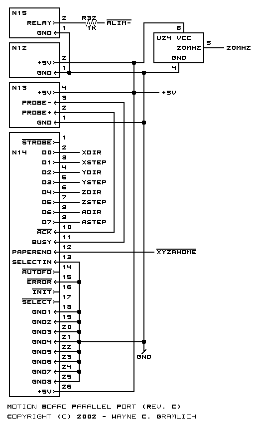
The parallel port schematic is shown below:
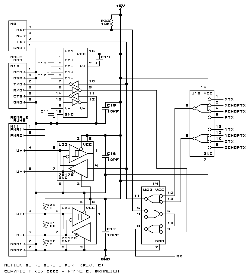
The serial port schematic is shown below:
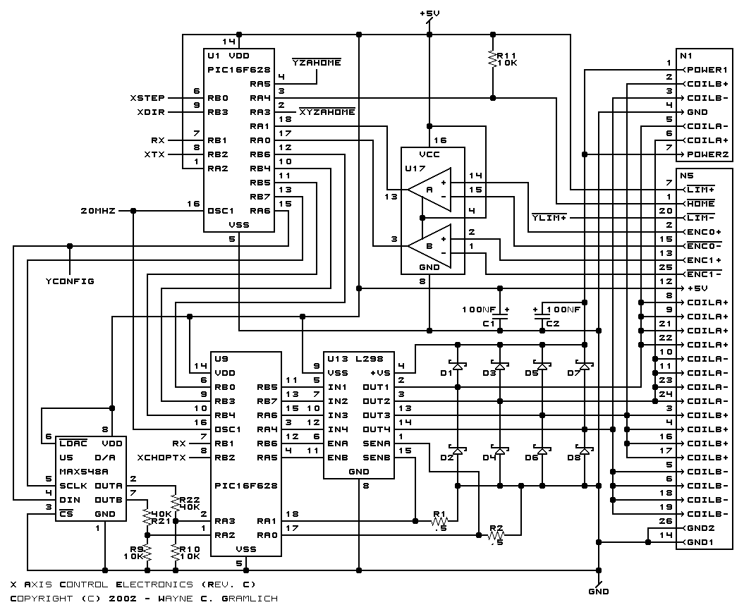
The X Axis schematic is shown below:
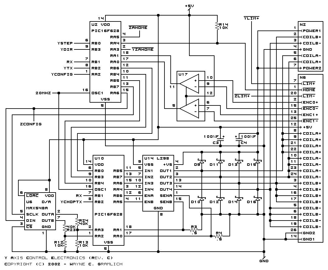
The Y Axis schematic is shown below:
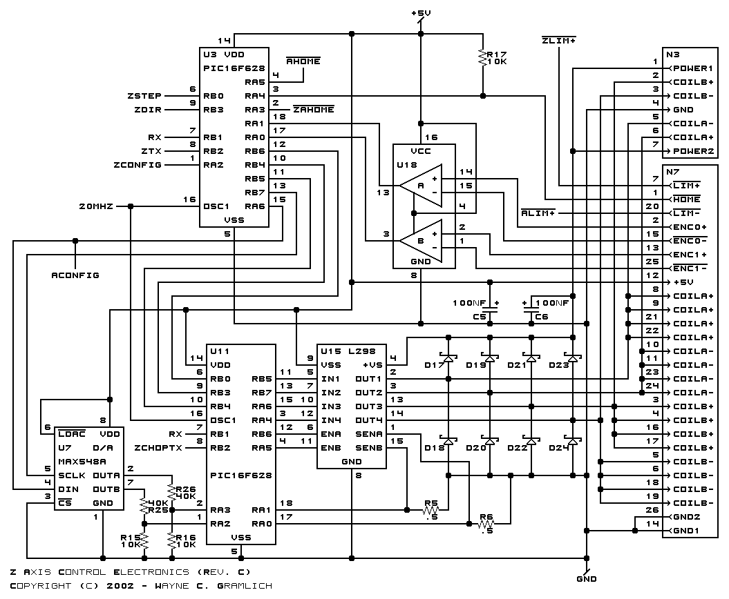
The Z Axis schematic is shown below:
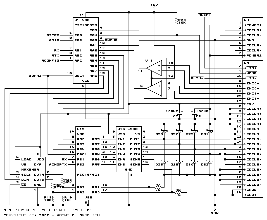
The A Axis schematic is shown below:
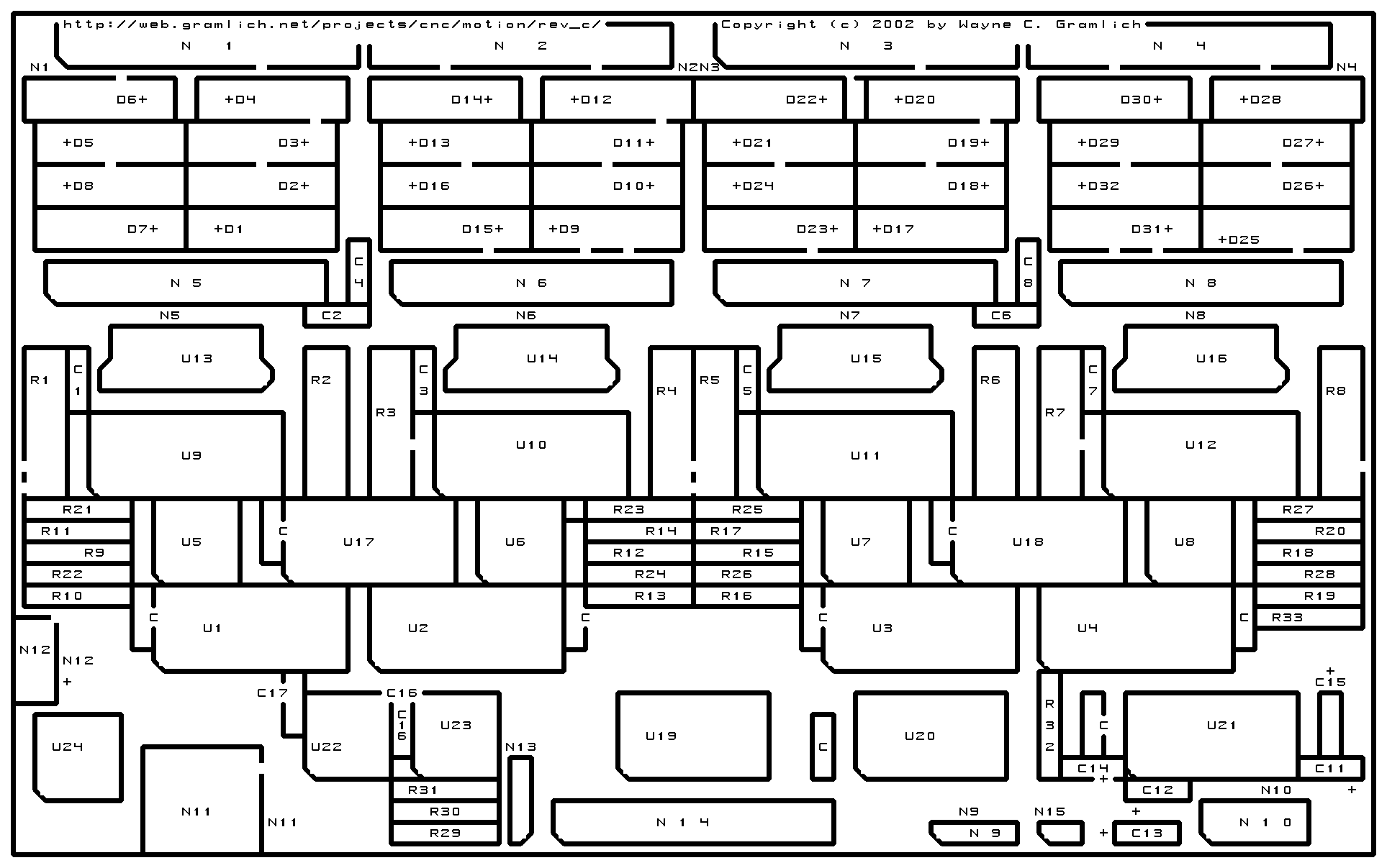
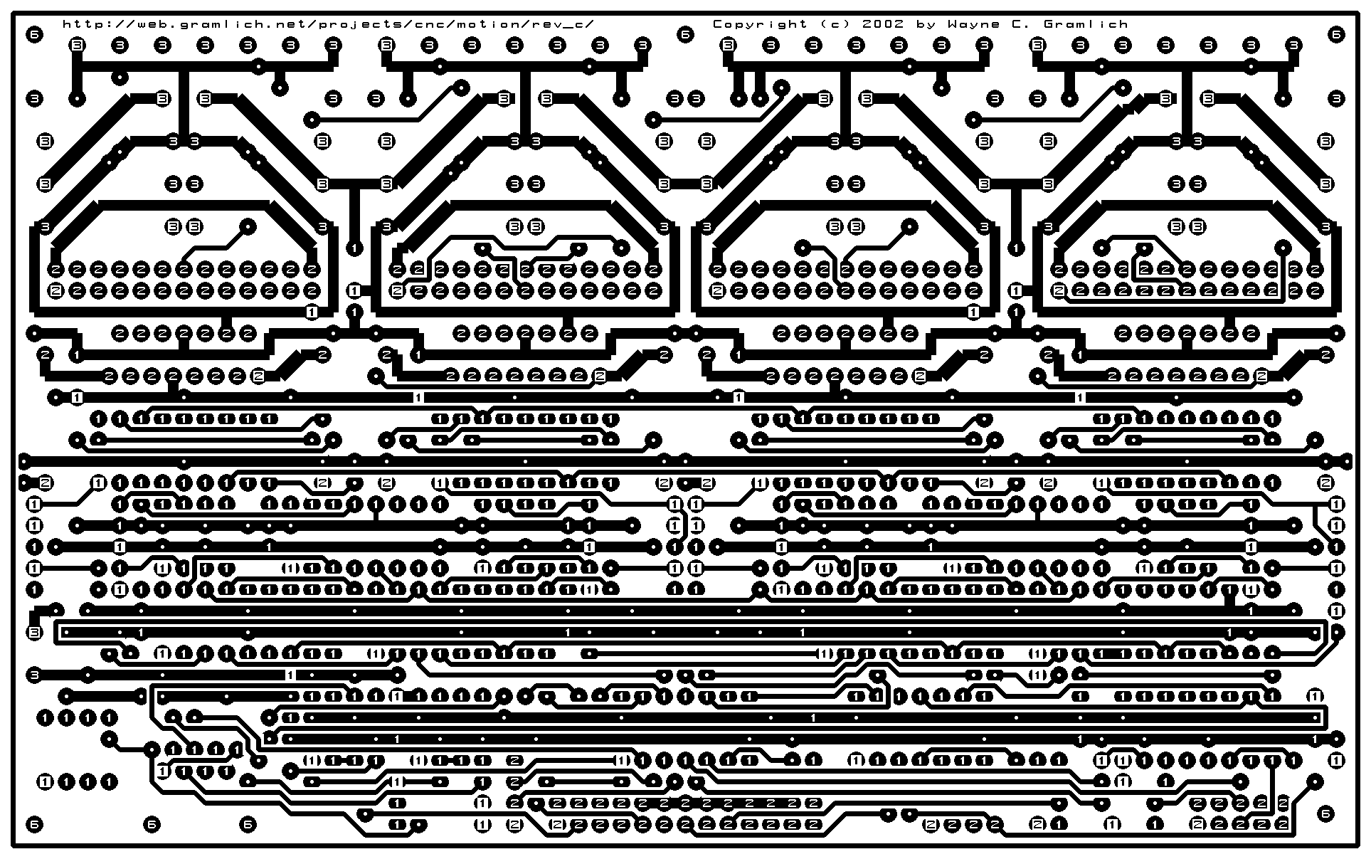
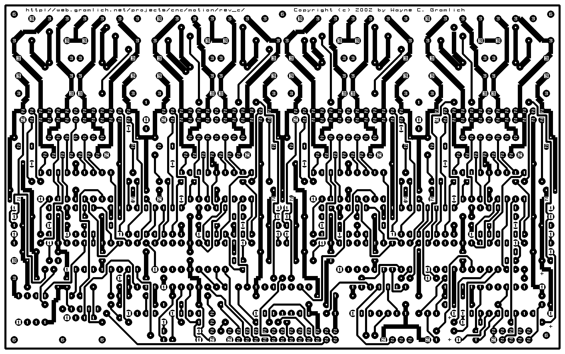
The printed circuit board files are listed below:
Any fabrication issues go here.