This is part of the MRNet project.
The purpose of the layout control mother board is to provide a simple way to allow people to control portions of their layout. The layout control motherboard consists of a single microcontroller that interfaces to the MRNet bus and a number of slots into which inexpensive control and sensor boards can be plugged in. All of the control and sensor boards share the single microcontroller on the motherboard.
The sensor and control boards that plug into the layout control mother board are meant to be quite inexpensive. The interface circuitry that must be on each control and sensor card consists of 1 74LS14 Hex Schmitt Trigger (Jameco 46640 @ $.25 ea) and 1 74LS165 8-bit shift register (Jameco 46877 @ $.49 ea). The motherboard provides regulated 5 volts to each board using a simple 7805 based power supply. In addition, the boards are provided unregulated positive and negative voltages that can be used to switch relays and the like.
The currently available control and sensor boards are:
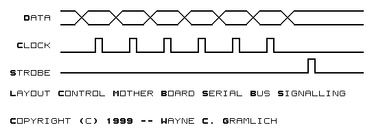
The controller talks to the control and sensor boards via a simple 4 wire bus. Each board implements a long shift register of 8-bit bytes. The output of control and sensor board is directed to the input of the next sensor board. The output of the last sensor board is automatically routed back to the microcontroller for reading. A simple clock line is used to shift the bits in all of the shift registers one bit over. Finally, there is a strobe line that is asserted by the microcontroller to indicate that it is done shifting data through the shift register. This strobe line is used to load data into and out of the shift register.
A quick and dirty diagram of the serial line protocol is shown below:
Actually, the signals are all active low, so the clock and strobe lines should be inverted.
The layout control mother board schematics is broken into the three schematics shown below:
The first schematic has the power supply and hub circuitry:
{Circuit description goes here.}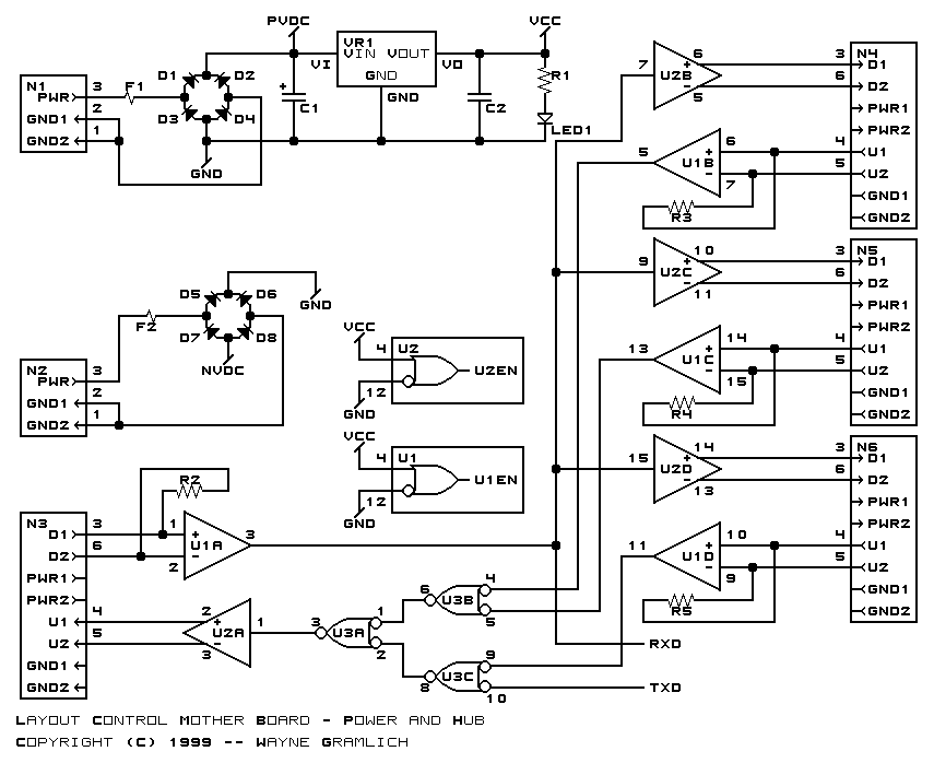
The second schematic shows the microcontroller connections:
{Circuit description goes here.}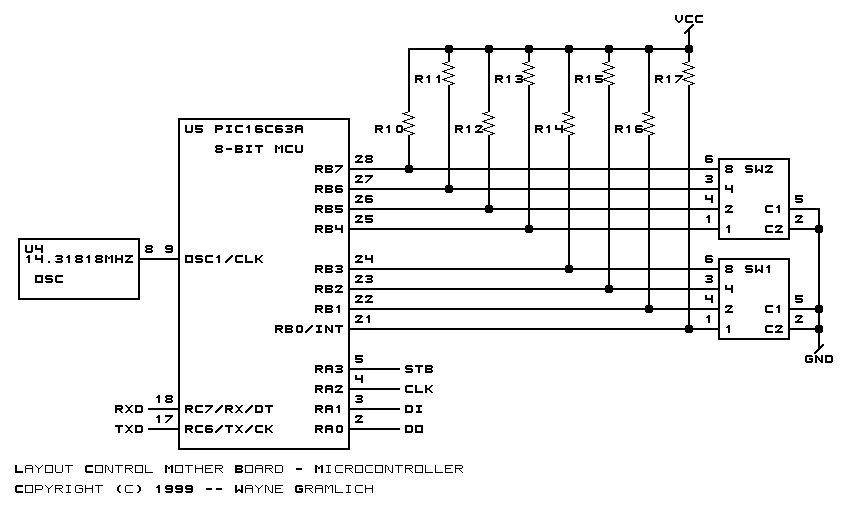
The third schematic shows the connector connections to the control and sensor boards:
{Circuit desciption goes here.}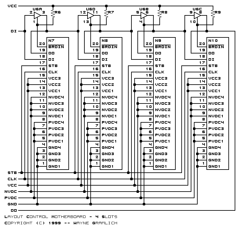
Every control and sensor board has one 74LS165 (8-bit parallel load serial shift register) that is used to provide identification information about the control and sensor board. The contents of this byte are described in the table below:
where
Bit 7 Bit 6 Bit 5 Bit 4 Bit 3 Bit 2 Bit 1 Bit 0 Id Inputs Outputs
By encoding the number of input and output bytes into the board indentification byte, it is possible for the microcontroller software to easily figure out the total shift register length and were each board is in the total shift register. This means that new control and sensor boards can be introduced after without having to update the microcontroller firmware.
The table below shows the identifier computation for four boards:
Name Id Inputs Outputs Id Byte Value (Hex) LED Card 0 0 4 04 Button Card 0 3 0 18 Bipolar Turnout Card 0 0 2 02 Block Card 0 2 0 10
The current design of the mother board uses .1 inch (2.54mm) dual row male headers for connectors (Jameco 53479 @ $.39 ea.) Each sensor board must have one female right angle .1" inch header to make the corresponding connection (Jameco 71829 @. $.49 ea.) The advatnage of these connectors is that they are quite standard and the are commonly available with gold plating. The disadvantage is that they do not have positive retention. To deal with the lack of positive retention, I have made it possible to add two little loops of wire next on each side of the female connector. There are corresponding holes next to each male header on the mother board. A simple screw and nut can be used to firmly attach the control and sensor boards to the mother board.
There are no predefined board dimensions for the control and sensor boards. The only requirement is that the female connector must be on the lower left of the board as shown below:
This allows two rows of boards to stick out in each direction from the motherboard as is shown in the diagram below: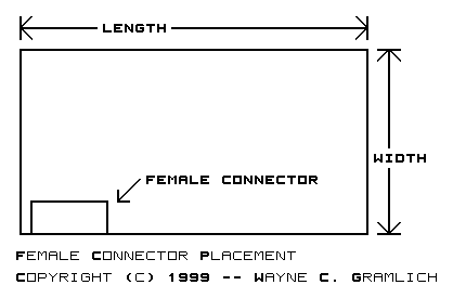
There can be a large number of wires going to and from each Layout Control Mother Board. If this board is stashed under the layout, there are going to be bunch of bumped heads getting under the layout. This amount of crawling under the layout can be reduced by making the layout control board easier to access. This can be accomplished by mounting the board on swivel standoffs (Jameco 143520 @ $.69 ea). By mounting the standoffs pointing down on the inside edge of the layout frame, it is possible to swing the board forward and down to work on the board and backward and up for operation. This is shown in the diagram below:
In order for the boards to swing freely, you should attempt to bring all of the cabling in at the pivit points. Alternatively, leave extra wire and provide a hook to hang the wire on. While you will still have to crawl under the layout to get install the wires for signal lights, turnout solenoids, and track power, once you run the wires to the front of your layout, you can do the remaining wire hookup out in front.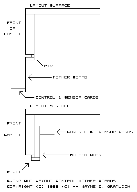
The layout control mother board has been layed out. The following are available: