
This is schemaitcs (and PCB) documentation for my CNC Axis4 control board revision A.
This Axis4 board provides 4 axes of stepper motor control. The current through the stepper motor coils is controlled via chopper technology. The maximum current is 2 Amperes. The controller supports 8× microstepping. Also, there is a 128K×8 static RAM buffer for buffering serial commands sent over a 115200 baud serial line from a host computer. The power supply is kept off board.
The parts list is kept in a separate file.
Since there are so many different "open source" licenses available, I have not yet decided which which "open source" license to release this 4 axis controller under. Thus, this controller is currently just copyrighted (ada I have all rights to it and you have none.) I have decided to defer the license selection decision until the first person comes along and says, "hey, I'd like to build one of these." If you want to build the project below, please contact me, Wayne C. Gramlich, and we can figure out the license issues together.
The power supply schematic is shown below:
The power supply is pretty mundane. The 110VAC comes in on connector N11 and is hooked in series with a power switch SW1, a fuse F1, and the primary coil of transformer T1. The secondary coil of T1 produces 24VAC at 12 Amps and is routed through the full wave bridge rectifier BR1 and onto the controller board at connector at pins 3 and 4 of N7. A large off-board filter capacitor of 10,000µF (C52) is connected to the controller board at pins 1 and 2 of N7. In addition, a 24VDC cooling fan is connected at pins 1 and 2 of N8. Resistor R12 and red LED D5 will bleed off the charge of C52 when power is turned off. As long as D5 is lit, there is charge on the capacitor and extra care should be taken. The 24V primary coil is rated in RMS (Root Mean Squared), so the actual peak voltage is 24V/.707 or approximately 35 volts. The unregulated voltage is used by the stepper and selenoid drivers as VDC. The unregulated voltage is stepped down through VR1, VR2 and VR3 to produce the 5 volts needed by the digital circuitry. The reason for using 3 voltage regulators is because 1) the stepper motors and selenoid chopper circuits will be causing a fair amount of roughness on the unregulated voltage and 2) the amount of heat generated will be spread across 3 voltage regulators rather than just 1. While the schematic does not show it, there are test points for each of the voltage regulators on the PCB. Lastly, power on is indicated by the green LED D6 which is current limited by R10. LED D6 is mounted off board on the chasis.
The microcontroller1 schematic is shown below:
Microcontroller 1 (U11) is used to manage the serial input from the host computer. It consists of a 40-pin PIC16F777-I/P microcontroller running at 20MHz (X1). It communicates with the host processor by receiving serial data in on RXD (pin 26) and transmitting serial data on TXD (pin 25). All received data is temporarily strored into the static RAM. This is done using the M0-7 (pins 33-40), ADRL (pin 15), ADRM (pin 16), A16-18 (pins 2-4), OE (pin 23) and WE (pin 24). Using the data from the host computer the, microcontoller is repsonsible for strobing the stepper motors using the A/X/Y/Z STEP/DIR lines (pins 19-22, 27-30).
If the user wishes to use the parallel port (N6) instead of the serial port, this microcontroller is not installed.
The microcontroller2 schematic is shown below:
Microncontoller 2 (U12) is a 40-pin PIC16F777-I/P responsible for processing the step signals from either the parallel port (N6) or microcontroller 1 (U18). It runs at 20MHz using resonator X2. The emergency stop and/or limit switches are connected to N9. If there is any break in the circuit, resistor R13 will pull the MCLR (pin 1) to zero and freeze the microcontroller in the reset state. In short order, this causes all of the H-bridges to become unpowered. The step signals come in on A/X/Y/Z STEP/DIR (pins 2-9). The X and Y H-Bridge polarities are set via X1-X4 (pins 19-22) and Y1-Y4 (pins 27-30). The A and Z H-bridge polarities are set via Z1-Z4 (pins 33-36) and A1-A4 (pins 37-40). The STB signal (pin 15) is used to trigger all 4 H-bridges on.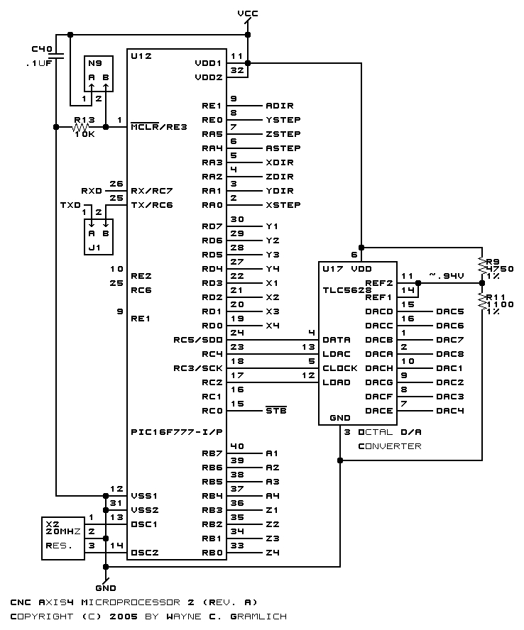
U17 is an 8-channel 8-bit serial D/A converter. It is connected to the SPI clock (pin 18) and SPI data (pin 24) on the microcontroller. The LOAD signal (pin 17) causes the current serial command to be loaded into U17. The LDAC signal (pin 23) causes the buffered voltage values to be placed out on DAC1-DAC8 (pins 1-2, 7-10, 15-16). The maximum allowed voltage is set via REF1-2 (pins 11, 13) is approximately 0.94 volts. Using the .51 ohm current sense resistors, this works out to just under 2 amperes of current. The 0.94 volts is set by the R9 and R11 voltage divider.
The serial port schematic is shown below:
The serial port is a standard 9-pin D connector hooked up for serial communication using RS-232 voltage levels (±12 volts). A standard MAX-232 level converter chip is used. C44-C47 are 1 µF capacitors needed for the charge pump.
The parallel port schematic is shown below:
The parallel port uses a 25-pin D connector. D0-D7 are used for the A/X/Y/Z STEP/DIR signals on pins 2-9. Ground is connected to pins 18-25.
The static RAM is a 128K×8, 256K×8, or 512K×8 memory chip that resides in a 32-pin DIP package. The pin-outs for these chips are listed in the table below. The only pins that are different between the three chips are pin 1 (A18) and pin 30 (CS2/A17).
Pin 128K×8 256K×8 512K×8 1 NC NC A18 2 A16 A16 A16 3 A14 A14 A14 4 A12 A12 A12 5 A7 A7 A7 6 A6 A6 A6 7 A5 A5 A5 8 A4 A4 A4 9 A3 A3 A3 10 A2 A2 A2 11 A1 A1 A1 12 A0 A0 A0 13 DQ0 DQ0 DQ0 14 DQ1 DQ1 DQ1 15 DQ2 DQ2 DQ2 16 Vss Vss Vss 17 DQ3 DQ3 DQ3 18 DQ4 DQ4 DQ4 19 DQ5 DQ5 DQ5 20 DQ6 DQ6 DQ6 21 DQ7 DQ7 DQ7 22 CE CE CE 23 A10 A10 A10 24 OE OE OE 25 A11 A11 A11 26 A9 A9 A9 27 A8 A8 A8 28 A13 A13 A13 29 WE WE WE 30 NC(CS2) A17 A17 31 A15 A15 A15 32 Vcc Vcc Vcc
The static RAM memory schematic is shown below:
An 8-bit bus named M0-7 is connected between microcontroller 1 and the static RAM sub-system. This bus can be used to store 16-bits of address into 8-bit latches U13-14, store 8-bits of data into the memory chip U15, or read 8-bits of data from U15. The ADRM line is used to latch one latch of 8 address bits. The ADRL line is used to latch the other 8 address bits. The WE (pin 29) and OE (pin 24) lines are used to read and write data into U15. The more or less random connections between address lines, latches, M bus and data I/O pins on U15 are all dictated by PCB layout issues. Remember, memory chips are symetric in address and data, so any data and/or address lines can be exchanged without effecting functionality.
The X Axis schematic is shown below:
The bipolar stepper motor is connected to connector N1. Connector N1 is connected to the L298 (U1) dual H-Bridge IC and and the octal Schottky diode (D1). The Schottky diodes ensure that the voltage to the H-Bridge never exceeds VDC + 0.2V or -0.2V. There are six 470µF capacitors (C1-6) attached to VDC help even out some of the power fluctuations that result from chopping. Capacitory C7 is a .1µF capacitor to filter out high frequency noise from switching.
The chopping occurs by pulse width modulation of the enable inputs for the L298 (pins 6, 11). When the enabled, voltage is applied to one end of each coil and ground to the other. The direction of current flow through a stepper motor coil is set by X1:X2 and X3:X4.
The amount of current flowing through each coil is sensed using the .51 Ohm sense resistors R1-2. Since the maximum allowed current is 2 Amperes, the maximum voltage is 1.0 volts. At maximum current, the resistor is consuming 2 Watts of power (i.e. 1V × 2A = 2W). Thus, R1-2 are 2 watt resistors. The resistors must not be wound wire resistors.
The sensed voltage is fed into 1/2 of a LM339 quad comparator. Whenever the sense resistor voltage exceeds the voltage present on DAC1-2, the comparator goes low; this causes the appropriate flip-flop in U5 to turn off, which, in turn, disables the H-bridge.
The H-bridge is turned on by asserrting the flip flop preset (pins 4, 10) low. This signal is held low until after any spurious pulses from the sense resistors have died down. The STB signal should be between 20KHz and 30KHz.
The Y Axis schematic is shown below:
The Y axis is the same as the X axis above, with different component labels.
The Z Axis schematic is shown below:
The Z axis is the same as the X axis above, with different component labels.
The A Axis schematic is shown below:
The A axis is the same as the X axis above, with different component labels.
The printed circuit board files are listed below:
The following fabrication issues came up: