This is the Revision A version of the
PIC876Hub10 RoboBrick. The status of this project is
that it has been
replaced by the
Revision B version.
PIC876Hub10 Robobrick (Revision A)
This document is also available as a
PDF document.
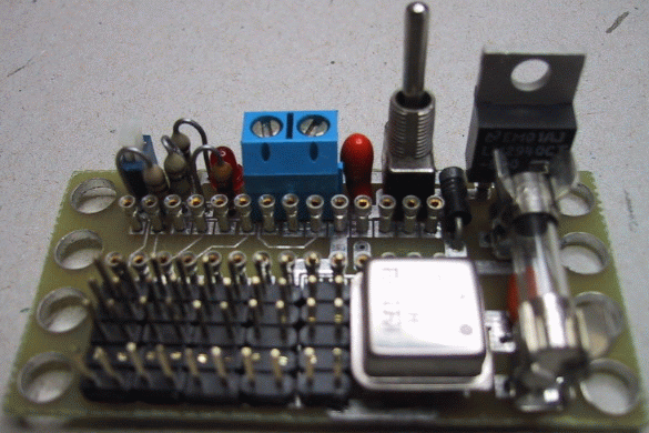
The PIC876Hub10 RoboBrick is a master RoboBrick that
can control up to N slave RoboBricks. It uses a
PIC16F876 microcontroller from
MicroChip®. One of the hub
ports can be connected to a communications RoboBrick
to provide the ability to talk to the development
platform.
There is a three terminal connector, one for ground
and the other two for power. One power connector
is connected to a standard 3-terimal 5 volt regulator
to provide 5 volts to the slave RoboBricks. The
other power regulator is only sensed for voltage
level. The microcontroller has a built in analog
to digital converter that allows it to sense the
power level on both power terminals. When the power
goes below a preset level, the robot platform can
choose to enter a `hungry' behavior mode.

There is no programming specification for the PIC876Hub10
RoboBrick yet.
The hardware consists of a circuit schematic and
a printed circuit board.
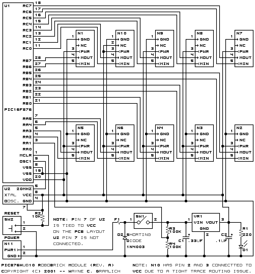
The schematic for the PIC876Hub10 RoboBrick is shown below:

The parts list kept in a separate file --
pic876hub10.ptl.
The printed circuit board files are listed below:
-
pic876hub10_back.png
-
The solder side layer.
-
pic876hub10_front.png
-
The component side layer.
-
pic876hub10_artwork.png
-
The artwork layer.
-
pic876hub10.gbl
-
The RS-274X "Gerber" back (solder side) layer.
-
pic876hub10.gtl
-
The RS-274X "Gerber" top (component side) layer.
-
pic876hub10.gal
-
The RS-274X "Gerber" artwork layer.
-
pic876hub10.drl
-
The "Excellon" NC drill file.
-
pic876hub10.tol
-
The "Excellon" tool rack file.
There is no software for this RoboBrick yet.
The following fabrication issues came up:
-
The holes for N1-N10 (size 3) are too
large and should be made smaller (size 2).
-
Label the components in the upper right
corner better.
-
Think about making the holes for SW1 (size 4)
a bit larger (size 5).
-
The fuse is too long, make it .10 inches
or .15 inches shorter.
-
Think about rearranging the switch to be
a little higher up to get further away
from the heat sink on VR1.
-
Look around for an alternative processor
the has reprogrammable flash. They should
be starting to arrive on the scene.
-
Put a plus sign next to the appropriate
terminal of D1.
-
Put a plus sign next to the appropriate
terminal of D2.
-
Put a 1 next to the appropriate terminal
of U2.
-
Look for another more PCB friendly power
switch.
-
Look for a better push button.
-
Put a plus sign next to the appropriate
terminal of C1.
-
Try to find room for another terminal
on N1 and two resistors to build a second
battery voltage divider.
-
Think about adding a heart beat LED.
-
Move U2 down .05 inches so it does not
interfere with N10.
-
The crystal interfers with N10.
-
The reset button may not be needed.
Copyright (c) 2001-2002 by
Wayne C. Gramlich.
All rights reserved.
