This is the Revision A verion of the
Harness RoboBrick. The status of this project is
that it has been
replaced by the
Revision C version.
Harness Robobrick (Revision B)
This document is also available as a
PDF document.
The Harness RoboBrick is used to test a
RoboBrick network. It is built using a PIC16F84
microcontroller from
MicroChip. The PIC16F84 is used so that the
software can easily be changed for testing purposes.
Either a dumb terminal or a terminal emulator is
connected to the Harness RoboBrick via a
Tether RoboBrick. Communication occurs at
2400 baud.
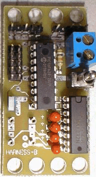
A picture of Harness-B is shown below (without the
crystal):

The Harness commands are summarized as follows:
-
N
s -
Send a single byte containing N
(where N is an octal number)
to the RoboBrick. Do not wait for any
reply bytes.
-
N
w -
Send a single byte containing N
(where N is an octal number) to
the RoboBrick. The program waits for up
to 5 response bytes. If no byte is
present, the byte 376 is returned. All
returned bytes are printed as 3-digit
octal numbers.
-
i -
Interrogate the RoboBrick to find out its
identification information.
The hardware consists of a circuit schematic and
a printed circuit board.
The schematic for the Harness RoboBrick is shown below:

The parts list kept in a separate file --
Harness.ptl.
The printed circuit board files are listed below:
-
harness_back.png
-
The solder side layer.
-
harness_front.png
-
The component side layer.
-
harness_artwork.png
-
The artwork layer.
-
harness.gbl
-
The RS-274X "Gerber" back (solder side) layer.
-
harness.gtl
-
The RS-274X "Gerber" top (component side) layer.
-
harness.gal
-
The RS-274X "Gerber" artwork layer.
-
harness.drl
-
The "Excellon" NC drill file.
-
harness.tol
-
The "Excellon" NC drill rack file.
The Harness software is available as one of:
-
harness.ucl
-
The µCL source file.
-
harness.asm
-
The resulting human readable PIC assembly file.
-
harness.lst
-
The resulting human readable PIC listing file.
-
harness.hex
-
The resulting Intel® Hex file
that can be fed into a PIC12C5xx programmer.
The following fabrication issues came up:
-
Make the holes of N1 and N2 (size 3) smaller
(size 2).
-
Put a 1 next pin one of the crystal.
-
Think about making the holes of S1
(size 4) larger (size 5).
-
Increase the spacing between the capacitors.
-
Add a low pass filter capacitor for U1.
-
This board needs to be layed out again!
It is seriously bungled!
-
Add a couple of heart beat LED's.
-
Find a better reset button; or just leave
a 2-pin male header.
-
Add a power on LED.
-
Add a pin 1 next to the DB9 connector.
-
It is hard to insert and remove the PIC16F628;
either switch over to in-circuit programming,
or move the chip to one edge.
-
The crystal can is grounded; be careful not
to push the crystal all the way in, or it
might ground either the power or signal wire.
Use crystals with longer leads.
Copyright (c) 2000-2002 by
Wayne C. Gramlich.
All rights reserved.
