This is Revision A of the Extensible Multiple Device Programmer 3 and it is currently a work in progress.
The EMDP4 base consists of 5 broad sections:
- Power Supply
- The power supply takes power from 24 VDC wall transformer and breaks it into 24V, 12V, 8V, and 5V.
- 5-Volt Microcontroller
- The 5 volt microcontroller interfaces to the RS-232 serial connector and the USB-B connector. It is also responsible for talking to the checker, controlling the status LED's and setting the voltage for the LOW voltaage microcontroller.
- Low Voltage Microcontroller
- The low voltage microcontroller is run at the voltage level appropriate for programming the device to be programmed. It has direct control over a 24V DAC and a 8V DAC.
- Customization Plug
- The customization plug is just a large number of female pins for routing power and signals to the 40-pin ZIF socket. One half of the customization plug is hooked to the low voltage microcontroller.
- 40-pin ZIF Socket
- The 40-pin ZIF socket is connected to the other half of the customization plug. The first 9 pins of the ZIF socket are connected to ICSP connector.
The parts list is kept in a separate file.
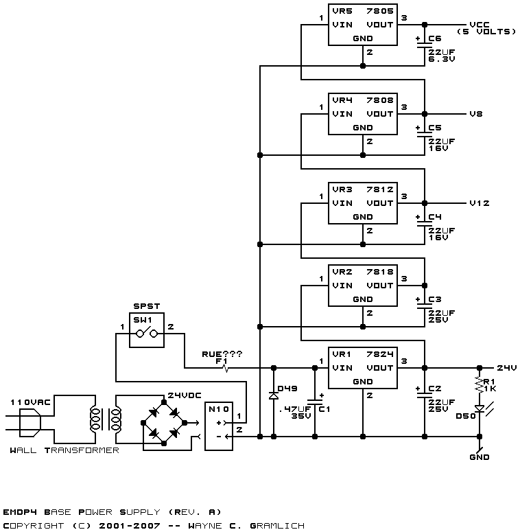
The power supply circuit diagram is shown below:
The power supply uses a Underwriters Labratory® approved "wall wart" to provide 24VDC of power. This means that the base board does not have any 110 AC or such voltages running around on it. The power comes in on either N1 (on board) or N3 (off board). The power switch can either be on board at SW1 or off board as SW2 through connector N2. A resettable polyswitch fuse is used to deal with short circuits at F1. D1 is a shorting diode that should trigger F1 if somehow a VAC power source gets plugged into N1 or N3.
The rest of the power supply a series of inexpensive linear voltage regulators, VR1-VR5, that step the voltage from 24 volts, to 18 volts, to 12 volts, to 8 volts and finally to 5 volts. All of these supplies are used elsewhere on the board except the 18 volt one, which is used to keep the 24 volt regulator, VR1, from disapating too much heat. The capacitors are tantalum for their low series resistance. This design will not win any energy conservation awards, but since the EMPD3 should spend 99% of its time turned off, there should be no real complaints. Finally, green LED D2 lights up to indicate that the device is turned on.
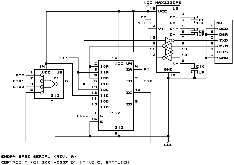
The serial communications circuit diagram is shown below:
The EMDP4 is a board that uses standard serial communcations protocols. Connector N6 is used connect to a DB9 port on a host computer that uses RS-232 voltage levels for signalling. U7 in conjunction with C7 through C10 converts the RS-232 levels to 5 volt levels. Connector N7 uses a RJ45 jack to provide RS-422 using SimpliciNet pin outs. The nifty DS8921AT at U10 provides RS-422 to 5 volt signalling level conversions.
U9A OR's the recevied signal from U7 or U10 and forwards the signal to the slave microcontroller (U1), the master microcontroller (U2), and to some gating circuitry that potentially gates the signal onto one of the bi-directional bus lines.
U9B OR's the transmit signals from the slave microcontroller (U1), the master microcontroller (U2), and through some gating logic with U8, potentially one of the bi-directional bus; the OR'd signal is forwarded to both the RS-422 connector and RS-232 connector.
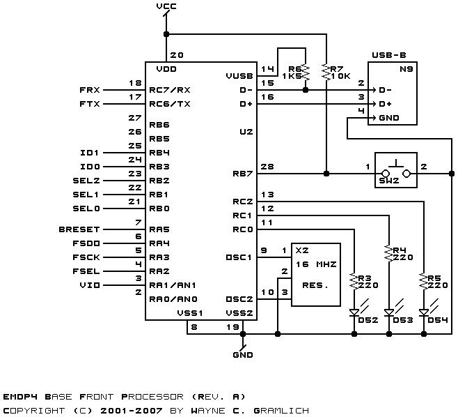
The co-processor circuit diagram is shown below:
The front processor is responsible for managing the EMDP4 base board. It consists of a PIC16F628, U1, ...
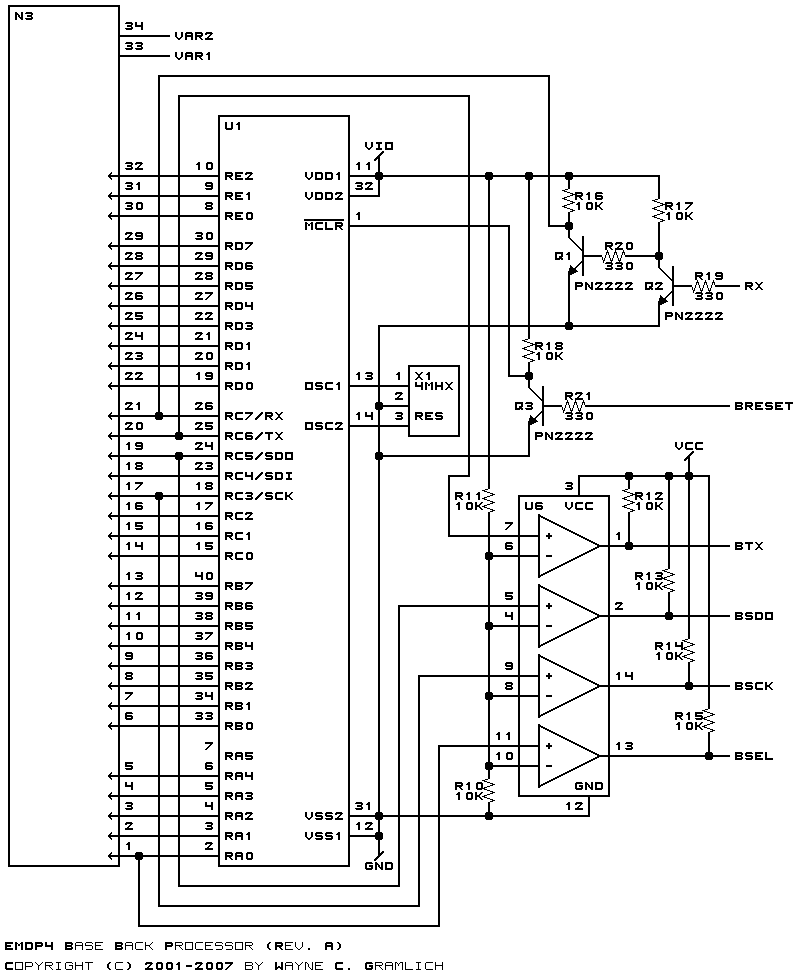
The low voltage processor circuit diagram is shown below:
U1 is the back processor is a low-voltage PIC16LF877. This microcontroller has direct access to all 30 of the bidirectional lines. The remaining two lines are LVPRX for serial data recieve, LVPTX for serial data transmit. The adaptor boards can be connected to the bus via the 37-pin female D connector N4.
Upon startup, the coprocessor is in charge. It immediately asserts LVPRESET# to force the low voltage processor into the reset state. Eventually, it will get around to setting VIO to the correct voltage and will release LVPRESET#. After that, the low voltage processor initializes itself and forces the bus lines to high impedance. Next, the programming algorithm is downloaded over the serial lines LPVRX and LVPTX.
There is one buttons, SW2 that can be read by the coprocessor. SW2 is used to initiate programming from the programmer.
Lastly, the STB signal is on RA5 of microcontroller U1. This pin has an open collector output an needs to be pulled high by R21. The data coming back from the IDDAT line is pulled high by R22 to detect when there is now adaptor/plug connected to the system.
The Digital to Analog converters circuit diagram is shown below:
The digital to analog converter is implemented by U15, a serial quad 8-bit D/A. All of the reference voltages are tied to 2.5 volts. D/A output A is used to generate VAR1, a 0 to 24 output in .1 volt increments. D/A output B is used to generate a 0 to 10 volt output in .05 volt increments. D/A output C is used to genarate a 0 to 8 volt output in increments of .05 volts.
All three amplifiers are the same basic design with different resistor values to change the over gain. A transistor is in the feedback circuit to provide additional current capacity.
Alas, none of the PCB work has even been started.
The following printed circuit board files are available:
Any fabrication issues will be listed here.