
This is Revision C of the Extensible Multiple Device Programmer and it is currently a work in progress.
This is revision D of the EMDP1 mother board. It differs from revision C in that power supply has been simplified to use a 24-volt wall wart and some inexpensive linear voltage regulators instead of the more complicated switching supply.
The parts list is kept in a separate file.
The schematic for the power supply is shown below:
The power supply takes its power from a 24-volt VDC wall wart either via N1, an on board connector, or via N10 an off-board connector. The power switch is either mounted on board or off-board via connector N2. The fuse can either be on board at F1 or off board via connector N3. Diode D1 is a shorting diode that should short the supply and burn out the fuse if the power supply gets hooked up backwards. The 24VDC is regulated to 24 volts via C1, U1, and C2. The 24Volts is regulated down to 15 volts via U2 and C3. The 15 volts is regulated down to 5 volts vis U3 and C4. N? is available if people wish to provide an source of power supply voltages and leave U1-U3 empty.
The schematic for the serial communication is shown below:
The EMDP1 can communicate with its host processor via either RS-232 or RS-422 signaling. The RS-232 signaling takes place via an industrys standard female DB9 connector. The RS-422 signaling done via an RJ45 connector using standard Cat5 (catagory 5) cabling. The RS-422 is wired to conform to my SimpliciNet `standard', which allows both RS-422 signalling and power over the same cable. The RS-232 signals are converted to logic levels using U3, a standard MAX232 level convert chip. U4 is an RS-422 transceiver configured as an RS-422 transmitter and U5 is an RS-422 transceiver configured as a receiver. Resister R7 is 100 ohms of RS-422 termination and R8 and R9 provide biasing resistors to ensure that a logic high level is output if now RS-422 signal is present. U6A is takes the logical or of the received signals from the RS-232 and RS-422 and sends them on to the microcontroller serial receive line. U6B logically or's the transmit signals from the adaptor (via U11A) or from the microcontroller (MTX). R27 is forces the adaptor signal out if the microcontroller chip is being programmed by the bootstrap adaptor.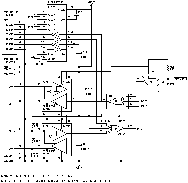
The schematic for the processor is shown below:
The U7 microcontroller is a Microchp® PIC16F877. U8 is a 20MHz crystal oscillator chip to provide the required clock signal. Connector N8 and resistor R6 is an optional reset button circuit. Jumper N11 shorted when the bootstrap adaptor is being used to program the microcontroller. Connector N7 is a 40-pin connector that is connected to a 37-pin D connector. In addition, the exact same signals are routed to N13 of the `universal' plug.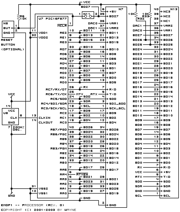
The schematic for 40-pin ZIF (Zero Insertion Force) socket is shown below:
The ZIP socket N15 has a direct wiring between its pins and the other half of the `universal' plug N14.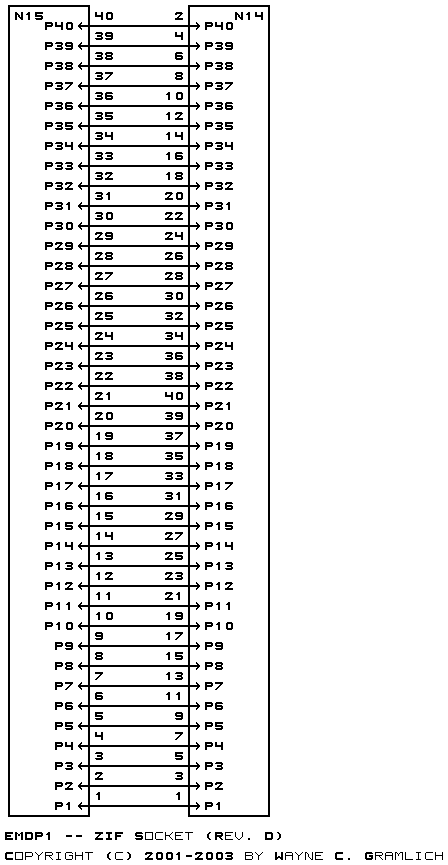
The schematic for the Digital to Analog converters is shown below:
The microcontroller controls the digital to U10 analog converter using standard I2C signalling. The D/Aconverter is a MAX518. (I'm quite nervious about the continued availabilty of this chip; most I2C chips are being manufactured in surface mount packages only.) Resistors R28 and R29 are the required pull-up resistors for I2C. The outputs of the MAX518 is run into two op amps in U9 configured as linear amplifiers to take the 0 to 5 volt output swing of the D/A and convert it 0 to 24 volt swing. The capacitors C12 and C13 prevent overshoot. Connector N12 is used by the bootstrap adaptor to get 24 volts of power to feed back to the microcontroller at 13 volts for programming purposes.
The following printed circuit board files are available:
Any fabrication issues will be listed here.