This is revision A of the PIC_Serial Adaptor Board and it is currently a abandoned. It has been replaced by Revision B.
This version of the PIC Serial adaptor did not work out and was replaced by Revision B. Only continue reading if you like seeing what my original thoughts were.
This document is also available in PDF format.
The PIC Serial Adaptor Board is used to program Microchip PIC microcontrollers using one of their serial programming protocols.
In order to serially program a PIC, 5 Volts (Vdd), 13 Volts (Vpp), Ground, Clock and Data need to be routed to the appropriate pins on the chip.
This adaptor board directly supports the PIC microcontrollers that are in 8, 14, 18, 28, and 40 pin DIP (Dual Inline Package) packages. Any surface mount PIC microcontrollers will need an alternative adaptor; since I am perfectly happy to use DIP packaging for all of my projects that use PIC microcontrollers, I am in no particular hurry to design an adaptor for surface mount PIC chips.
My going in design decision was that there was going to be a single 40-pin ZIF (Zero Insertion Force) socket and that I would always place pin 1 of each PIC microcontroller in the upper left corner of that socket, irrespective of whether the chip is in an 8, 14, 18, 28, or 40 pin DIP package. The table below summerizes my investigations regarding which PIC chips require which voltages and signals on which pins. If the chip is in a in 40-pin package, the pin numbers are straight forward. For 8, 14, 18, and 28 pin packages, any pin which falls on the right side of the package has its corresponding location on the 40-pin socket listed in parenthesis. For example, for the PIC16F62x, pin 20 on the 28-pin chip corresponds to pin 32 on the 40-pin chip. The table is listed immediately below:
Proc. Class Pkg. Clk. Data Vpp Vdd (+5V) Vss (Gnd) LVP Class A A 28/40 39 40 1 11, 32 8, 12, 31 36 16F62x A 28 27 (39) 28 (40) 1 20 (32) 8,19(31) 24 (36) 16F64x/66x, 16C6x/7x/9x, 16F7x A 28/(40) 27 (39) 28 (38), 26 (40) 1 20 (32) 8,19 (31) - 16C6x/7x/9x, 16F64x/66x A 40 39 40 1 11,32 12,31 - 16F87x A 40 39 40 1 11,32 12,31 36 16F7x A 40 39 40 1 11,32 12,31 - Class B B 8/14 38 39 4 1 40 - 12C5xx,12C67x B 8 6 (38) 7 (39) 4 1 8 (40) - 16C505 B 14 12 (38) 13 (39) 4 1 14 (40) - Class C C 18 34 35 4 36 5 32 16C6x/7x/9x, 16C715,
16C84, 16F8x, 16C55xC 18 12 (34) 13 (35) 4 14 (36) 5 - 16F62x C 18 12 (34) 13 (35) 4 14 (36) 5 10 (32) 16C432 - 20 13 (33) 14 (34) 5 15 (36) 6 - 16C433 - 18 12 (34) 13 (35) 8 5 2,3,14(36),16(38) - 14000 - 28 12 11 13 9 20 (32) - Union ? 40 12, 33, 34, 38, 39 11, 34, 35, 38, 39, 40 1, 4, 5, 8, 13 1, 5, 9, 11, 32, 36 2, 3, 5, 6, 12, 31, 32, 36, 38, 40 32, 36 All Pins ? ? 1, 2, 3, 4, 5, 6, 8, 9, 11, 12, 13, 31, 32, 33, 34, 35, 36, 38, 39, 40
What I discovered is that most of the PIC chips fell into three broad classes, called imaginatively enough class A, B, and C. Given that I already use PIC microcontrollers in each class, I want it easy to flip between the classes.
My original thought was to have a separate personality plug for each class. As I figured out how big a connector I was going to need, that did not seem like such a good idea. I ultimately decided to assign a 2×10 male header to each class. A simple shorting plug that shorts across the header to configure each class. The PIC microcontrollers that do not fall into one of these three classes will need a speciallized plug that plugs into all 3 class plugs and a fourth leftover plug. This seems like a reasonably trade-off between ease of use and flexibility.
One final requirement for the class plug is that I want the software in the EMDP1 to be able to determine which plug has been activated. There requires some plug identification lines that feed back to the EMDP1.
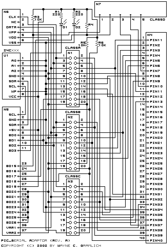
The schematic for this revision is shown below:
When I was trying to lay out the board, it was taking up much more space than I wanted. Eventually, I decided my idea of having a larger plug was not such a bad idea after all. The files for the incomplete printed circuit board are listed below:
Since this design was never complete, the likelyhood of it being fabricated is zero. Hence, there will not ever be any fabrication issues to list here.