This is revision A of the EPROM Adaptor Board and it is currently a work in progress.
The EPROM adaptor is used to program the 27C080, 27C040, 27C020, 27C010, 27C512, 27C256, 27C128, 27C64, 2732, and 2716. (The venerable 2708 requires an extra -5V bias voltage, so we do not support that chip.)
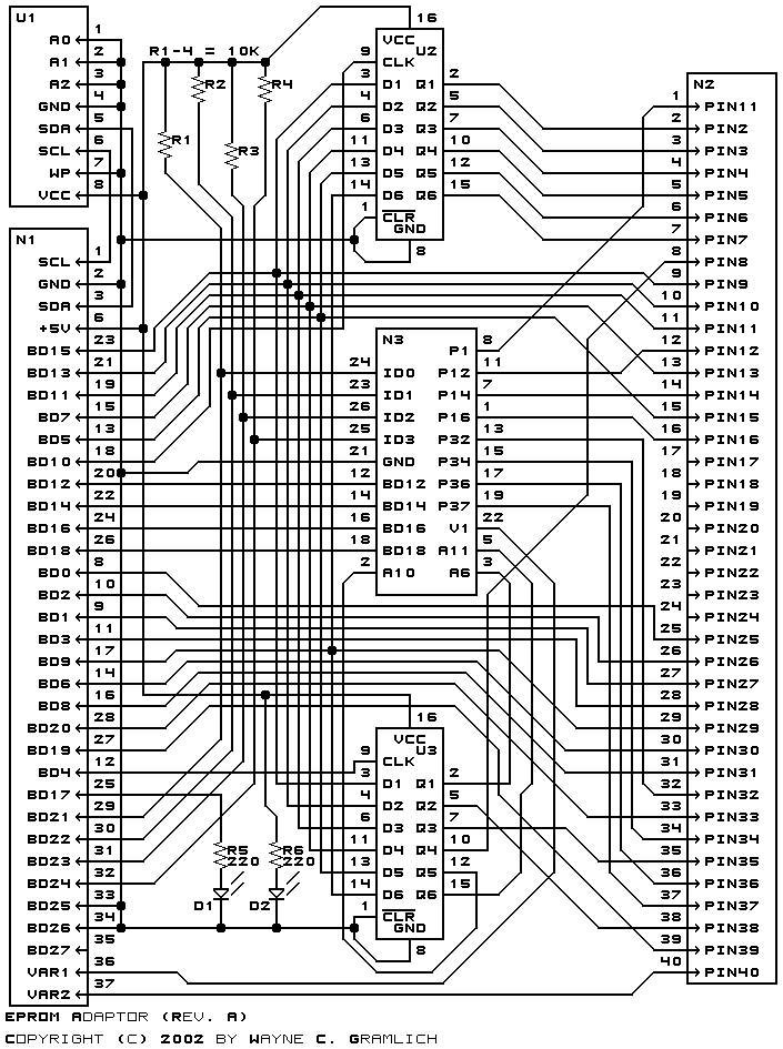
The schematic for this revision is shown below:
Note, the pin assignments were all picked to make the board layout easy. Thus, the seemingly random order of some of the pin assignments.
The N1 connector is assigned as follows:
Pin Name Connected To 1 SCL U1-SCL 2 GND Ground 3 SDA U1-SDA 4 5 6 +5V Vcc 7 8 BD0 ZIF40 Pin 25 9 BD1 ZIF40 Pin 27 10 BD2 ZIF40 Pin 26 11 BD3 ZIF40 Pin 28 12 BD4 Strobe A6-A11 13 BD5 ZIF40 Pin 15; U2-A4; U3-A10 14 BD6 ZIF40 Pin 30 15 BD7 ZIF40 Pin 13; U2-A3; U3-A9 16 BD8 ZIF40 Pin 31 17 BD9 ZIF40 Pin 29; U2-A5; U3-A11 18 BD10 Strobe A0-A5 19 BD11 ZIF40 Pin 11; U2-A2; U3-A8 20 BD12 Plug BD12 21 BD13 ZIF40 Pin 10; U2-A1; U3-A7 22 BD14 Plug BD14 23 BD15 ZIF40 Pin 9; U2-A0; U3-A6 24 BD16 Plug BD16 25 BD17 Program LED 26 BD18 Plug BD18 27 BD19 ZIF40 Pin 39 28 BD20 ZIF40 Pin 33 29 BD21 Plug ID0 30 BD22 Plug ID1 31 BD23 Plug ID2 32 BD24 Plug ID3 33 BD25 Ground 34 BD26 Ground 35 BD27 36 VAR1 Plug V1 37 VAR2 ZIF40 Pin 40 38 39 40
The plug, N3, has its pin assignments as shown below:
Pin Name Connected To 1 P16 ZIF40 Pin 16 2 A10 U3-A10 3 A0 U3-A6 4 5 A11 U3-A11 6 7 P14 ZIF40 Pin 14 8 P1 ZIF40 Pin 1 9 10 11 P12 ZIF40 Pin 12 12 BD12 N1-BD12 13 P32 ZIF40 Pin 32 14 BD14 N1-BD14 15 P34 ZIF40 Pin 34 16 BD16 N1-BD16 17 P36 ZIF40 Pin 36 18 BD18 N1-BD18 19 P37 ZIF40 Pin 37 20 21 GND Ground 22 V1 N1-VAR1 23 ID1 N1-BD22 24 ID0 N1-BD21 25 ID2 N1-BD23 26 ID3 N1-BD34
There are a total of 12 address bits that are latched. 11 of them are used. The table below shows where all the address bits go:
Name Loaded From Connected To Strobe A0 N1-BD15 ZIF40 Pin 2 N1-BD10 A1 N1-BD13 ZIF40 Pin 3 N1-BD10 A2 N1-BD11 ZIF40 Pin 4 N1-BD10 A3 N1-BD7 ZIF40 Pin 5 N1-BD10 A4 N1-BD5 ZIF40 Pin 6 N1-BD10 A5 N1-BD9 ZIF40 PIn 7 N1-BD10 A6 N1-BD15 Plug A6 N1-BD4 A7 N1-BD13 ZIF40 Pin 38 N1-BD4 A8 N1-BD11 ZIF40 Pin 35 N1-BD4 A9 N1-BD7 ZIF40 Pin 8 N1-BD4 A10 N1-BD5 Plug A10 N1-BD4 A11 N1-BD9 Plug A11 N1-BD4
The following printed circuit board files exist:
Any fabrication issues will be listed here.